
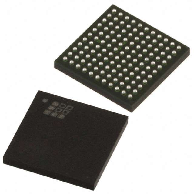
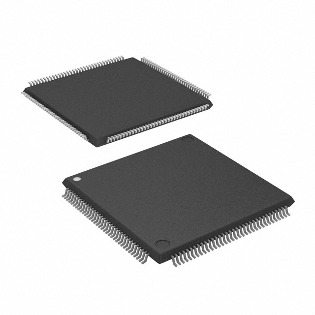
LFSC3GA40E-6FFAN1020C
對比
LFSC3GA40E-6FFAN1020C
IC FPGA 562 I/O 1020BGA


對比
面議
價格更新:一個月前
現貨供應:
3657


45
為45個國家的客戶提供服務
1000+
全球製造商
$140M
5年增長1.4億美元
50.0M+
5年內配送了5000萬個元件

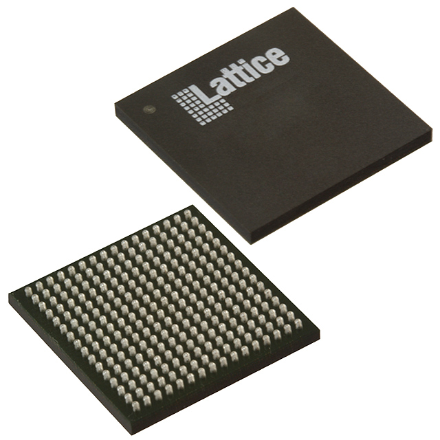
Lattice Semiconductor Corporation
Lattice Semiconductor 是低功耗可編程的領導者。 在不斷增長的通信、計算、工業、汽車和消費市場中,他們通過網絡解決客户問題,從邊緣到雲端。 他們的技術、長期合作關係以及對世界級支持的承諾讓他們的客户能夠快速、輕鬆地釋放他們的創新,以創造一個智能、安全和互聯的世界。
查看所有産品從 Lattice Semiconductor Corporation


The LatticeSC family of FPGAs combines a high-performance FPGA fabric, high-speed SERDES, high-performance I/Os and large embedded RAM in a single industry leading architecture. This FPGA family is fabricated in a state of the art technology to provide one of the highest performing FPGAs in the industry. This family of devices includes features to meet the needs of today���s communication network systems. These features include SERDES with embedded advance PCS (Physical Coding sub-layer), up to 7.8 Mbits of sysMEM embedded block RAM, dedicated logic to support system level standards such as RAPIDIO, SPI4.2, SFI-4, UTOPIA, XGMII and CSIX.
Feature
■ High Performance FPGA Fabric
• 15K to 115K four input Look-up Tables (LUT4s)
• 139 to 942 I/Os
• 700MHz global clock; 1GHz edge clocks
■ 4 to 32 High Speed SERDES and flexiPCS™ (per Device)
• Performance ranging from 600Mbps to 3.8Gbps
• Excellent Rx jitter tolerance (0.8UI at 3.125Gbps)
• Low Tx jitter (0.25UI typical at 3.125Gbps)
• Built-in Pre-emphasis and equalization
• Low power (typically 105mW per channel)
• Embedded Physical Coding Sublayer (PCS) provides pre-engineered implementation for the following standards:
– GbE, XAUI, PCI Express, SONET, Serial RapidIO, 1G Fibre Channel, 2G Fibre Channel
■ 2Gbps High Performance PURESPEED™ I/O
• Supports the following performance bandwidths
– Differential I/O up to 2Gbps DDR (1GHz Clock)
– Single-ended memory interfaces up to 800Mbps
• 144 Tap programmable Input Delay (INDEL) block on every I/O dynamically aligns data to clock for robust performance
– Dynamic bit Adaptive Input Logic (AIL) monitoring and control circuitry per pin that automatically ensures proper set-up and hold
– Dynamic bus: uses control bus from DLL
– Static per bit
• Electrical standards supported:
– LVCMOS 3.3/2.5/1.8/1.5/1.2, LVTTL
– SSTL 3/2/18 I, II; HSTL 18/15 I, II
– PCI, PCI-X
– LVDS, Mini-LVDS, Bus-LVDS, MLVDS, LVPECL, RSDS, Hypertransport
• Programmable On Die Termination (ODT)
– Includes Thevenin Equivalent and low power VTT termination options
■ sysCLOCK™ Network
• Eight analog PLLs per device
– Frequency range from 15MHz to 1GHz
– Spread spectrum support
• 12 DLLs per device with direct control of I/O delay
– Frequency range from 100MHz to 700MHz
• Extensive clocking network
– 700MHz primary and 325 MHz secondary clocks
– 1GHz I/O-connected edge clocks
• Precision Clock Divider
– Phase matched x2 and x4 division of incoming clocks
• Dynamic Clock Select (DCS)
– Glitch free clock MUX
■ Masked Array for Cost Optimization (MACO™) Blocks
• On-chip structured ASIC Blocks provide preengineered IP for low power, low cost system level integration
■ High Performance System Bus
• Ties FPGA elements together with a standard bus framework
– Connects to peripheral user interfaces for run-time dynamic configuration
■ System Level Support
• IEEE standard 1149.1 Boundary Scan, plus ispTRACY™ internal logic analyzer
• IEEE Standard 1532 in-system configuration
• 1.2V and 1.0V operation
• Onboard oscillator for initialization and general use
• Embedded PowerPC microprocessor interface
• Low cost wire-bond and high pin count flip-chip packaging
• Low cost SPI Flash RAM configuration


相關產品
| 製造商零件編號 | 價格(¥) | 現有數量 | |
|---|---|---|---|
 LFECP6E-3FN484CIC FPGA 224 I/O 484FBGA | 面議 |
2327
市場 |
產品屬性
| 類型 | 描述 | 全選 |
|---|---|---|
| 電壓 - 供電 | 0.95V ~ 1.26V | |
| 安裝類型 | 表面貼裝型 | |
| 系列 | SC | |
| 工作温度 | 0°C ~ 85°C(TJ) | |
| 包裝 | 託盤 | |
| 封裝/外殼 | 1020-BBGA,FCBGA | |
| 產品狀態 | 停產 | |
| 供應商器件封裝 | 1020-OFcBGA Rev 2(33x33) | |
| 可編程 | 未驗證 | |
| LAB/CLB 數 | 10000 | |
| 邏輯元件/單元數 | 40000 | |
| 總 RAM 位數 | 4075520 | |
| I/O 數 | 562 |
部落格
 芯能王電子有限公司祝您感恩節快樂感谢您成为芯能王电子大家庭不可或缺的一员,祝您感恩节快乐!
 探索 Nvidia H200 在 AI 模型訓練方面的強大功能使用Nvidia的H200芯片探索AI训练的尖端可能性。解锁您的AI模型的最终潜力,并彻底改变您的工作。
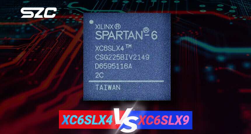 XC6SLX4 vs XC6SLX9:哪個更好?利用 XC6SLX4 和 XC6SLX9 FPGA 的潜力来增强性能和多功能性。
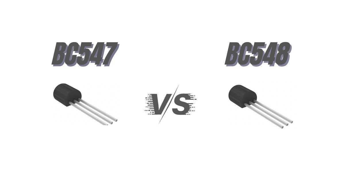
 美國十大微控制器製造商本文章主要介绍美国前十微控制器制造商。
 薄膜與陶瓷:選擇適合您的電容器当我们揭开薄膜和陶瓷电容器的神秘面纱时,探索电子元件的世界。在这个技术爱好者的指南中,系好安全带,通过电容电流进行迷人的旅程。

面議
價格更新:一個月前
現貨供應:
3657
Lattice Semiconductor Corporation
Lattice Semiconductor 是低功耗可編程的領導者。 在不斷增長的通信、計算、工業、汽車和消費市場中,他們通過網絡解決客户問題,從邊緣到雲端。 他們的技術、長期合作關係以及對世界級支持的承諾讓他們的客户能夠快速、輕鬆地釋放他們的創新,以創造一個智能、安全和互聯的世界。
查看所有産品從 Lattice Semiconductor Corporation部落格
- 芯能王電子有限公司祝您感恩節快樂感谢您成为芯能王电子大家庭不可或缺的一员,祝您感恩节快乐!
- 探索 Nvidia H200 在 AI 模型訓練方面的強大功能使用Nvidia的H200芯片探索AI训练的尖端可能性。解锁您的AI模型的最终潜力,并彻底改变您的工作。
- XC6SLX4 vs XC6SLX9:哪個更好?利用 XC6SLX4 和 XC6SLX9 FPGA 的潜力来增强性能和多功能性。
- 美國十大微控制器製造商本文章主要介绍美国前十微控制器制造商。
- 薄膜與陶瓷:選擇適合您的電容器当我们揭开薄膜和陶瓷电容器的神秘面纱时,探索电子元件的世界。在这个技术爱好者的指南中,系好安全带,通过电容电流进行迷人的旅程。
熱門製造商
View all manufactures 更多


熱門產品
更多電子零件 更多
ICE40LP384-SG32
IC FPGA 21 I/O 32QFN

LCMXO2-256HC-5SG32C
IC FPGA 21 I/O 32QFNS
ICE40HX1K-VQ100
IC FPGA 72 I/O 100TQFP
ICE40LP1K-CB121
IC FPGA 92 I/O 121CSBGA
ICE40HX4K-BG121
IC FPGA 93 I/O 121CABGA
LCMXO2-1200HC-6TG100C
IC FPGA 79 I/O 100TQFP
LIF-MD6000-6JMG80I
IC FPGA 37 I/O 80CTFBGA
LIA-MD6000-6JMG80E
IC FPGA 37 I/O 80CTFBGA
LCMXO3LF-6900E-6MG256C
IC FPGA 206 I/O 256CSFBGA
LCMXO2-7000HE-4TG144C
IC FPGA 114 I/O 144TQFP