
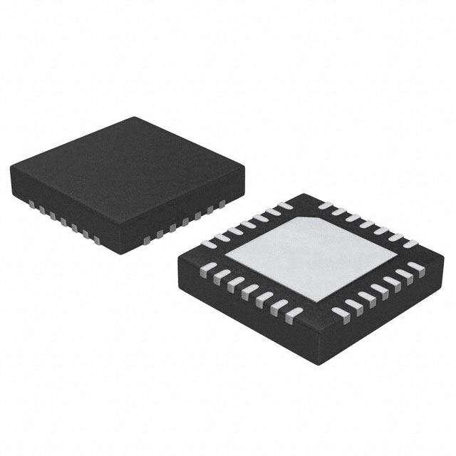
MAX11947GTP+T
對比
MAX11947GTP+T
4 CHANNEL AISG 3.0 COMPLIANT MOD
沒有數據表


對比


45
為45個國家的客戶提供服務
1000+
全球製造商
$140M
5年增長1.4億美元
50.0M+
5年內配送了5000萬個元件
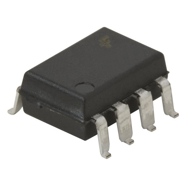
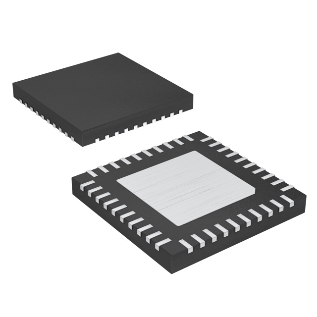
The MAX1190ECM is a 3.3V, dual 10-bit analog-to-digital converter (ADC) featuring fully differential wideband track-and-hold (T/H) inputs, driving two ADCs. The MAX1190ECM is optimized for low power, small size, and high-dynamic performance for applications in imaging, instrumentation, and digital communications. This ADC operates from a single 3.1V to 3.6V supply, consuming only 492mW while delivering a typical signal-to-noise and distortion (SINAD) of 57dB at an input frequency of 60MHz and a sampling rate of 120Msps. The T/H driven input stages incorporate 400MHz (-3dB) input amplifiers. The converters can also be operated with single-ended inputs. In addition to low operating power, the MAX1190ECM features a 3mA sleep mode, as well as a 1μA power-down mode to conserve power during idle periods. An internal 2.048V precision bandgap reference sets the full-scale range of the ADC. A flexible reference structure allows the use of this internal or an externally applied reference, if desired, for applications requiring increased accuracy or a different input voltage range. The MAX1190ECM features parallel, CMOS-compatible three-state outputs. The digital output format can be set to two's complement or straight offset binary through a single control pin. The device provides for a separate output power supply of 1.7V to 3.6V for flexible interfacing with various logic families. The MAX1190ECM is available in a 7mm x 7mm, 48-pin TQFP-EP package, and is specified for the extended industrial (-40°C to +85°C) temperature range. Pin-compatible lower speed versions of the MAX1190ECM are also available. Refer to the MAX1180–MAX1184 data sheets for 105Msps/80Msps/65Msps/40Msps. In addition to these speed grades, this family includes two multiplexed output versions (MAX1185/MAX1186 for 20Msps/40Msps), for which digital data is presented time-interleaved and on a single, parallel 10-bit output port. For lower speed, pin-compatible, 8-bit versions of the MAX1190, refer to the MAX1195–MAX1198 data sheets.
Feature
- Single 3.3V Operation
- Excellent Dynamic Performance
- 57dB SINAD at fIN = 60MHz
- 64dBc SFDR at fIN = 60MHz
- -71dBc Interchannel Crosstalk at fIN = 60MHz
- Low Power
- 492mW (Normal Operation)
- 10mW (Sleep Mode)
- 3.3μW (Shutdown Mode)
- 0.08dB Gain and 0.8° Phase Matching
- Wide ±1VP-P Differential Analog Input Voltage Range
- 400MHz -3dB Input Bandwidth
- On-Chip 2.048V Precision Bandgap Reference
- User-Selectable Output Format—Two's Complement or Offset Binary
- Pin-Compatible, Lower-Speed, 10-Bit and 8-Bit Versions Available
Applications
- Baseband I/Q Sampling
- Battery-Powered Instrumentation
- Multichannel IF Sampling
- Set-Top Boxes
- Ultrasound and Medical Imaging
- VSAT Terminals
- WLAN, WWAN, WLL, MMDS Modems


產品屬性
| 類型 | 描述 | 全選 |
|---|---|---|
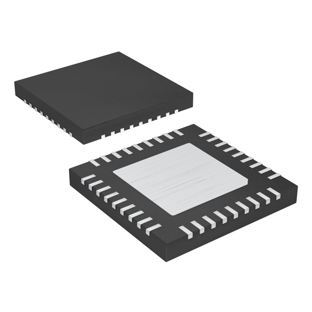
| 供應商 設備封裝 | 20-TQFN(4x4) | |
| 包裝 / 盒 | 20-WFQFN 裸露焊盤 | |
| 安裝類型 | 表面貼裝型 | |
| 輔助屬性 | 3V ~ 5.5V 電源 | |
| 射頻類型 | 通用 | |
| 功能 | 接收器 | |
| 產品狀態 | 在售 | |
| 包裝 | 卷帶(TR) |
¥42.76
價格更新:一個月前
現貨供應:
3935

Analog Devices Inc./Maxim Integrated
Maxim Integrated 現已成為 Analog Devices 的一部分。 它們相結合,提供了一套擴展的高性能混合信號和電源管理技術,幫助客户在各個市場取得成功。 其結果是提供了一系列解決最複雜問題的解決方案,從直流到 100 GHz,從納瓦到千瓦,從傳感器到雲。 在 Analog Devices 產品頁面上了解有關 Analog Devices 擴展產品組合的更多信息。
查看所有産品從 Analog Devices Inc./Maxim Integrated


部落格


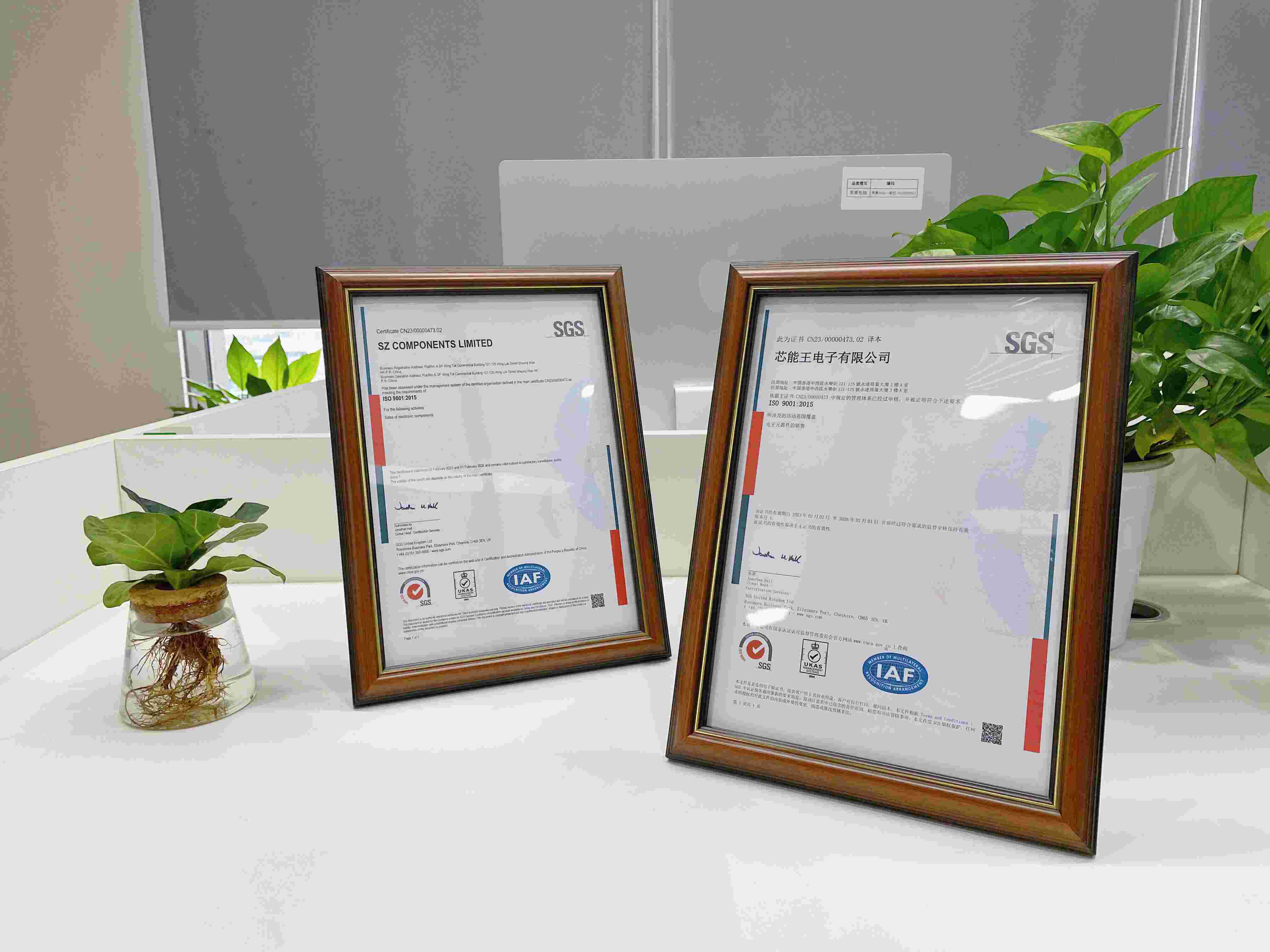 SZC自豪地宣佈通過ISO 9001:2015認證!SZC高兴地宣布,我们已成功获得ISO 9001:2015认证,这是一个重要的里程碑,彰显了我们对提供卓越质量和客户满意度的承诺。该认证证明了我们致力于持续改进,遵守行业标准,并在运营的各个方面不懈追求卓越。
 探索顏色傳感器在这篇综合文章中,我们将深入探讨什么是颜色传感器、它们的工作原理,以及为什么选择 SZComponents 来满足您的颜色传感器需求是一个您不会后悔的决定!那么,让我们一起踏上这段多彩的旅程吧。
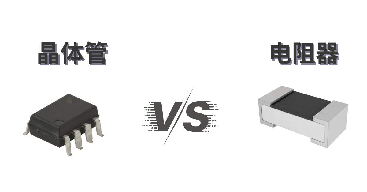 電晶體與電阻器:有什麼區別?在电子领域,晶体管和电阻器这两种重要元件发挥着独特但至关重要的作用。尽管尺寸不大,但这些元件却能够深刻地塑造电路和设备的行为。无论您是电子爱好者还是只是对技术感到好奇,了解晶体管和电阻器之间的差异都是一个很好的起点。
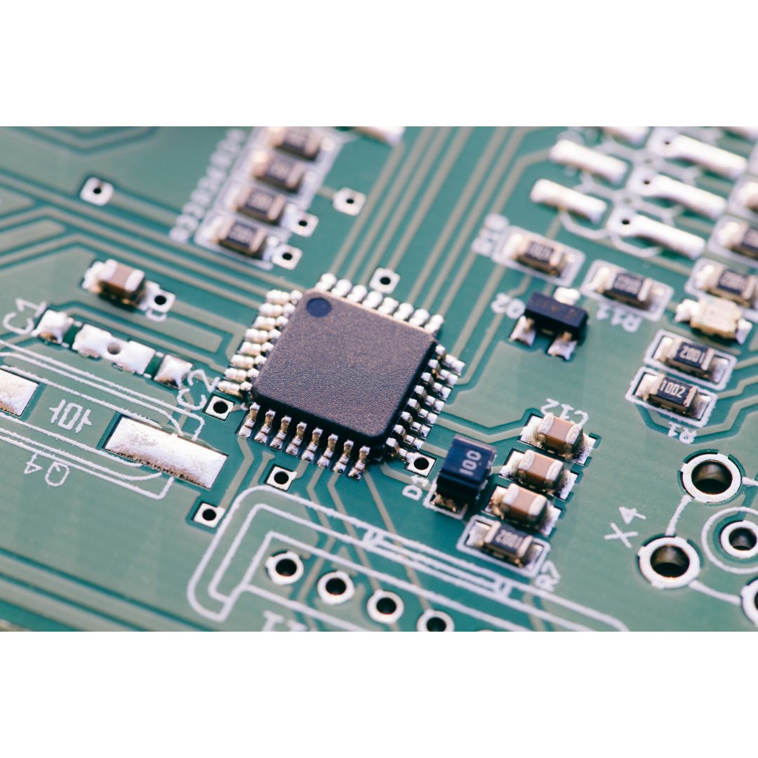 如何選擇微控制器?微控制器是大多数电子设备的支柱。它们是微型计算机,可以控制从微波炉到汽车发动机的一切。
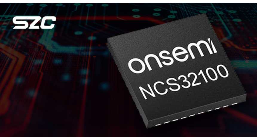 NCS32100:終極電感式傳感器接口使用NCS32100提升您的传感解决方案,NCS32100是一种电感式传感器,可为各种静态到高速操作提供高精度的角度读数。

熱門製造商
View all manufactures 更多


熱門產品
更多電子零件 更多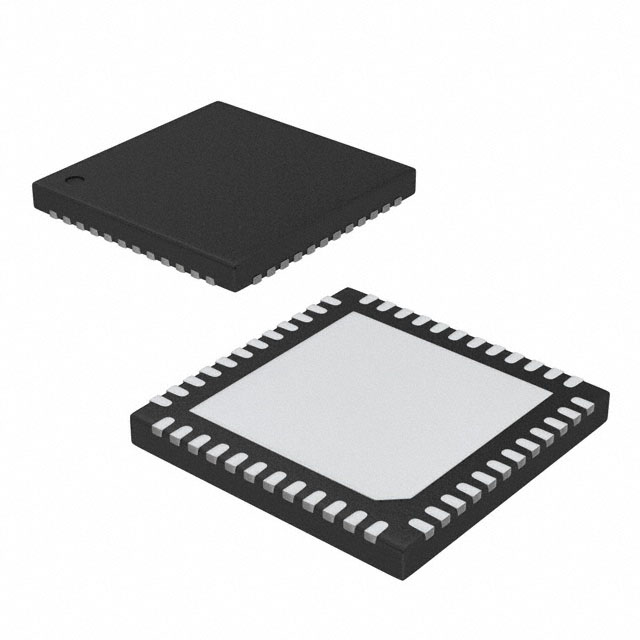
MAX11014BGTM+T
IC RF MESFET AMP 48TQFN

MAX2309ETI+
IC CDMA IF VGA/IQ DEMOD 28-TQFN
MAX2620EUA+
IC RF OSC W/BUFFERED OUT 8-UMAX
MAX2410EEI+
IC UP/DOWNCONVERTER 28-QSOP
MAX2021ETX+
IC MOD/DEMOD 36-TQFN

MAX2752EUA+
IC OSC VOLT CNTRL 8-UMAX
MAX1005CEE+
IC UNDERSAMPLER IF 16-QSOP
MAX2010ETI+
IC RF PREDISTORT ADJ 28-TQFN
MAX3805ETE
ADAPTIVE RECEIVE EQUALIZER
MAX2172ETL+
IC TUNER LOW IF CONV DGTL 40TQFN