


45
為45個國家的客戶提供服務
1000+
全球製造商
$140M
5年增長1.4億美元
50.0M+
5年內配送了5000萬個元件
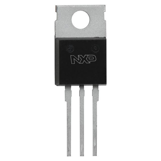
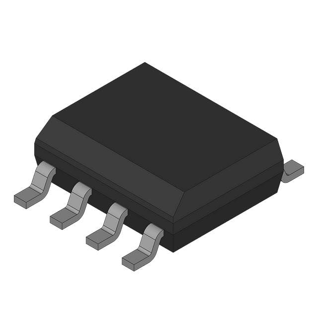
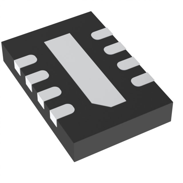
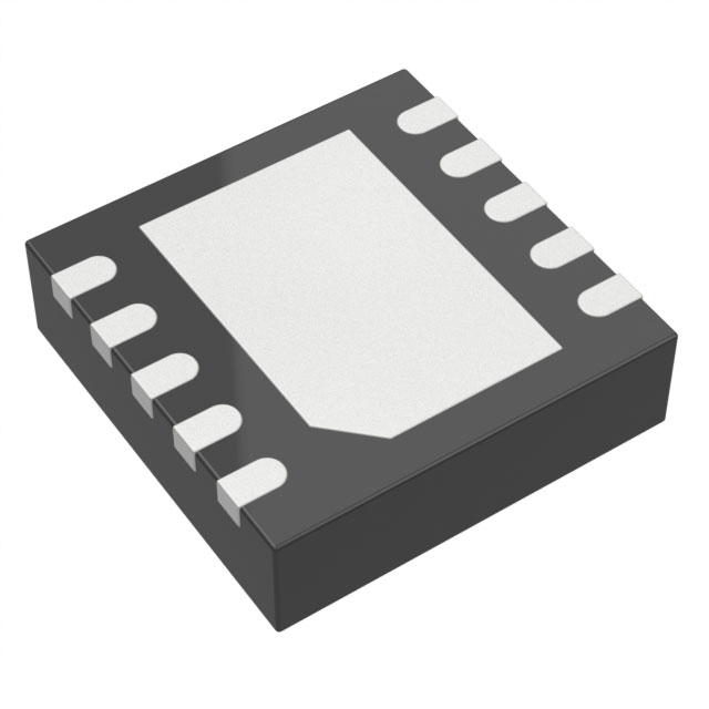
The ADL5906SCPZN-R7 is a true rms responding power detector that has a 67 dB measurement range when driven with a single-ended 50 Ω source. The easy to use input makes the ADL5906SCPZN-R7 frequency versatile by eliminating the need for a balun or any other form of external input tuning for operation up to 10 GHz.
The ADL5906SCPZN-R7 provides a solution in a variety of high frequency systems requiring an accurate rms measurement of signal power. The ADL5906SCPZN-R7 can operate from 10 MHz to 10 GHz and can accept inputs from −65 dBm to +8 dBm with varying crest factors and bandwidths, such as GSM-EDGE, CDMA, W-CDMA,TD-SCDMA, WiMAX, and OFDM-based LTE carriers. In addition, its temperature stability over the broad temperature range of −55°C to +125°C makes it ideally suited for a wide array of communications, military, industrial, and instrumentation applications.
Used as a power measurement device, VRMS is connected to VSET. The output is then proportional to the logarithm of the rms value of the input. In other words, the reading is presented directly in decibels and is scaled 1.1 V per decade, or 55 mV/dB; other slopes are easily arranged. In controller mode, the voltage applied to VSET determines the power level required at the input to null the deviation from the setpoint. The output buffer can provide high load currents.
Requiring only a single supply of 5 V and a few capacitors, it is easy to use and capable of being driven single-ended or with a balun for differential input drive. The ADL5906SCPZN-R7 has a low 250 µA sleep current when powered down by a logic high applied to the PWDN pin. It powers up within approximately 1.4 µs to its nominal operating current of 68 mA at 25°C.
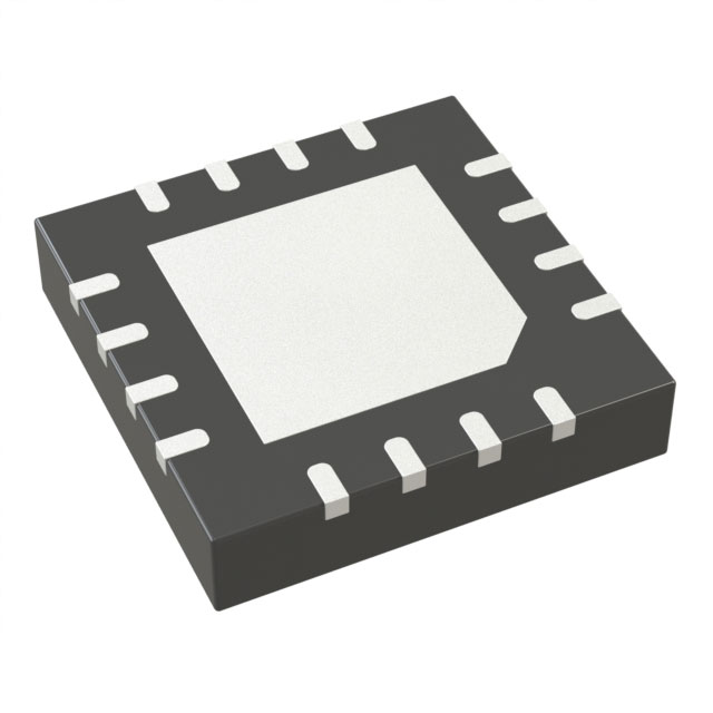
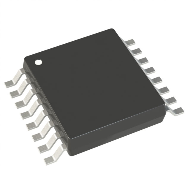
The ADL5906SCPZN-R7 is supplied in a 4 mm × 4 mm, 16-lead LFCSP and it is pin compatible with the ADL5902 and the AD8363 TruPwr™ rms detectors. This feature allows the designer to create one circuit layout for projects requiring different dynamic ranges. A fully populated RoHS-compliant evaluation board is available.
Feature
- Accurate rms-to-dc conversion from 10 MHz to 10 GHz
- Single-ended ±1 dB dynamic range: 67 dB at 2.14 GHz No balun or external input matching required
- Response independent of waveform types, such as GSM/CDMA/W-CDMA/TD-SCDMA/WiMAX/LTE
- Logarithmic slope: 55 mV/dB
- Temperature stability: <±1 dB from −40°C to +125°C
- Operating temperature: −55°C to +125°C
- Supply voltage: 4.75 V to 5.25 V
- Sleep current: 250 µA
- Pin-compatible withand
Applications
- Power amplifier linearization/control loops
- Transmitter signal strength indication (TSSI)
- RF instrumentation


相關產品
| 製造商零件編號 | 價格(¥) | 現有數量 | |
|---|---|---|---|
 ADL5906ACPZN-R7IC RF DETECT 10MHZ-10GHZ 16CSP | 62.00 |
1067
市場 | |
 ADL5903ACPZN-R7IC RF DETECT 868MHZ 8LFCSP | 30.00 |
2345
市場 | |
 ADL5611ARKZ-R7IC AMP W-CDMA 30MHZ-6GHZ SOT89-3 | 16.00 |
19136
市場 | |
 ADL5606ACPZ-R7IC AMP GPS 1.8GHZ-2.7GHZ 16LFCSP | 140.00 |
1101
市場 | |
 ADL5902ACPZ-R7IC RF DETECT 50MHZ-9GHZ 16LFCSP | 100.00 |
2000
市場 |
產品屬性
| 類型 | 描述 | 全選 |
|---|---|---|
| 安裝類型 | 表面貼裝型 | |
| 電流 - 供電 | 86 mA | |
| 電壓 - 供電 | 4.75V ~ 5.25V | |
| 精度 | ±1dB | |
| 射頻類型 | CDMA,GSM,LTE,WiMAX | |
| 頻率 | 10MHz ~ 10GHz | |
| 產品狀態 | 在售 | |
| 包裝 | 卷帶(TR) | |
| 系列 | TruPwr™ | |
| 供應商器件封裝 | 16-LFCSP(4x4) | |
| 封裝/外殼 | 16-WQFN 裸露焊盤,CSP |
¥280.00
價格更新:一個月前
現貨供應:
440

Analog Devices Inc.
Analog Devices(納斯達克股票代碼:ADI)是設計、製造和營銷廣泛的高性能模擬、混合信號和數碼訊號處理 (DSP) 集成電路 (IC) 產品組合的全球領導者,這些產品幾乎用於所有類型的 電子設備。 自 1965 年成立以來,他們一直專注於解決與電子設備信號處理相關的工程挑戰。 他們的信號處理產品已被全球超過 100,000 家客户使用,在將温度、壓力、聲音、光、速度和運動等現實世界現象轉換、調節和處理為電信號以用於廣泛應用方面發揮着重要作用 的電子設備。 Maxim Integrated 現在是 Analog Devices 的一部分。 結合起來,它們提供了一套擴展的頂級性能混合信號和電源管理技術,以幫助客户在日益數碼化、無處不在的感知和互聯世界中取得成功。 他們廣泛的工程能力和深度的領域專業知識共同幫助我們的客户解決從直流到 100 GHz、從納瓦到千瓦、從傳感器到雲的最複雜問題。
查看所有産品從 Analog Devices Inc.


部落格
 芯能王電子有限公司祝您感恩節快樂感谢您成为芯能王电子大家庭不可或缺的一员,祝您感恩节快乐!
 探索 Nvidia H200 在 AI 模型訓練方面的強大功能使用Nvidia的H200芯片探索AI训练的尖端可能性。解锁您的AI模型的最终潜力,并彻底改变您的工作。
 XC6SLX4 vs XC6SLX9:哪個更好?利用 XC6SLX4 和 XC6SLX9 FPGA 的潜力来增强性能和多功能性。
 美國十大微控制器製造商本文章主要介绍美国前十微控制器制造商。
 薄膜與陶瓷:選擇適合您的電容器当我们揭开薄膜和陶瓷电容器的神秘面纱时,探索电子元件的世界。在这个技术爱好者的指南中,系好安全带,通过电容电流进行迷人的旅程。


熱門製造商
View all manufactures 更多


熱門產品
更多電子零件 更多ADL5906SCPZN-R7
IC RF DETECT 10MHZ-10GHZ 16CSP
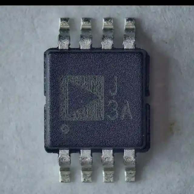
LTC5505-2ES5#TRMPBF
IC RF DETECT 300MZ-3.5GHZ TSOT23
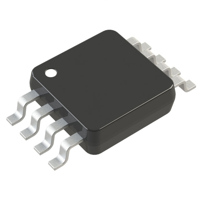
LTC5507ES6#TRMPBF
IC RF DETECT 100KHZ-1GHZ TSOT23
LT5581IDDB#TRMPBF
IC RF DETECT 10MHZ-6GHZ 8DFN
AD8361ARMZ-REEL7
IC RF DETECT 2.5GHZ 8MSOP

ADL5906ACPZN-R7
IC RF DETECT 10MHZ-10GHZ 16CSP
AD8314ARMZ
IC RF DETECT 100MHZ-2.7GHZ 8MSOP
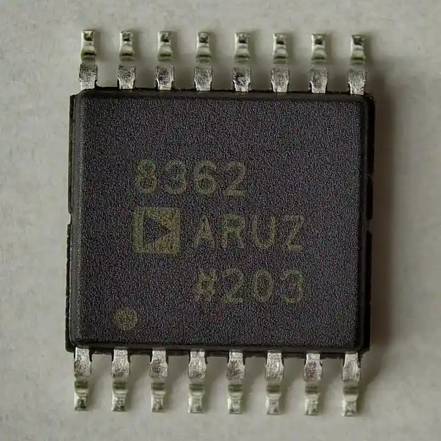
AD8362ARUZ-REEL7
IC RF DETECT 50HZ-3.8GHZ 16TSSOP
LTC5582IDD#PBF
IC RF DETECT 40MHZ-10GHZ 10DFN
AD8362ARUZ
IC RF DETECT 50HZ-3.8GHZ 16TSSOP