


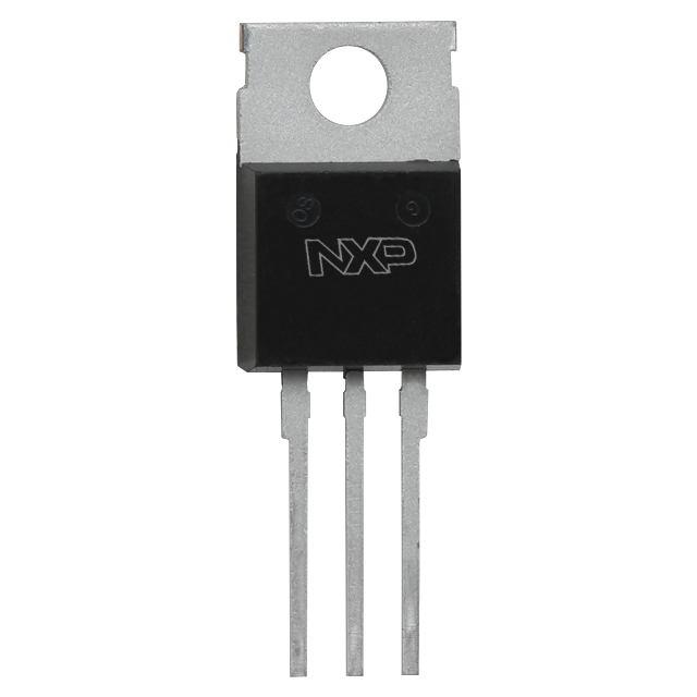
¥650.00
價格更新:一個月前
現貨供應:
500


45
為45個國家的客戶提供服務
1000+
全球製造商
$140M
5年增長1.4億美元
50.0M+
5年內配送了5000萬個元件

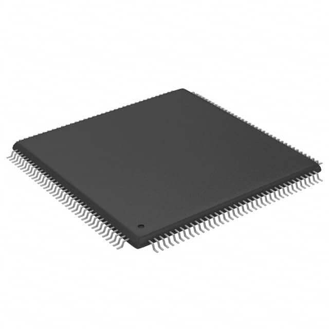
AMD
AMD是全可編程FPGA、SoC、MPSoC和3D IC的領先提供商。AMD獨特地實現了軟件定義和硬件優化的應用-推動了雲計算,5G無線,嵌入式視覺和工業物聯網領域的行業進步。
查看所有産品從 AMD


The CoolRunner-II 512-macrocell device is designed for both high performance and low power applications. This lends power savings to high-end communication equipment and high speed to battery operated devices. Due to the low power stand-by and dynamic operation, overall system reliability is improved This device consists of thirty two Function Blocks inter-connected by a low power Advanced Interconnect Matrix (AIM). The AIM feeds 40 true and complement inputs to each Function Block. The Function Blocks consist of a 40 by 56 P-term PLA and 16 macrocells which contain numerous configuration bits that allow for combinational or registered modes of operation. Additionally, these registers can be globally reset or preset and configured as a D or T flip-flop or as a D latch. There are also multiple clock signals, both global and local product term types, configured on a per macrocell basis. Output pin configurations include slew rate limit, bus hold, pull-up, open drain and programmable grounds.
A Schmitt-trigger input is available on a per input pin basis. In addition to storing macrocell output states, the macrocell registers may be configured as "direct input" registers to store signals directly from input pins. Clocking is available on a global or Function Block basis. Three global clocks are available for all Function Blocks as a synchronous clock source. Macrocell registers can be individually configured to power up to the zero or one state. A global set/reset control line is also available to asynchronously set or reset selected registers during operation. Additional local clock, synchronous clock-enable, asynchronous set/reset and output enable signals can be formed using product terms on a per-macrocell or per-Function Block basis. A DualEDGE flip-flop feature is also available on a per macrocell basis. This feature allows high performance synchronous operation based on lower frequency clocking to help reduce the total power consumption of the device. Circuitry has also been included to divide one externally supplied global clock (GCK2) by eight different selections. This yields divide by even and odd clock frequencies.
Feature
• Optimized for 1.8V systems
- As fast as 7.1 ns pin-to-pin delays
- As low as 14 μA quiescent current
• Industry’s best 0.18 micron CMOS CPLD
- Optimized architecture for effective logic synthesis
- Multi-voltage I/O operation — 1.5V to 3.3V
• Available in multiple package options
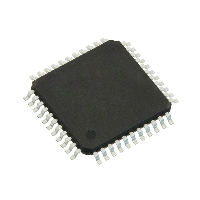
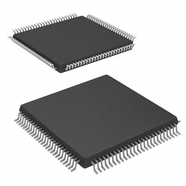
- 208-pin PQFP with 173 user I/O
- 256-ball FT (1.0mm) BGA with 212 user I/O
- 324-ball FG (1.0mm) BGA with 270 user I/O
- Pb-free available for all packages
• Advanced system features
- Fastest in system programming
· 1.8V ISP using IEEE 1532 (JTAG) interface
- IEEE1149.1 JTAG Boundary Scan Test
- Optional Schmitt-trigger input (per pin)
- Unsurpassed low power management
· DataGATE enable signal control
- Four separate I/O banks
- RealDigital 100% CMOS product term generation
- Flexible clocking modes
· Optional DualEDGE triggered registers
· Clock divider (divide by 2,4,6,8,10,12,14,16)
· CoolCLOCK
- Global signal options with macrocell control
· Multiple global clocks with phase selection per
macrocell
· Multiple global output enables
· Global set/reset
- Advanced design security
- PLA architecture
· Superior pinout retention
· 100% product term routability across function block
- Open-drain output option for Wired-OR and LED drive
- Optional bus-hold, 3-state or weak pullup on selected I/O pins
- Optional configurable grounds on unused I/Os
- Mixed I/O voltages compatible with 1.5V, 1.8V, 2.5V, and 3.3V logic levels
· SSTL2-1, SSTL3-1, and HSTL-1 I/O compatibility
- Hot Pluggable


相關產品
| 製造商零件編號 | 價格(¥) | 現有數量 | |
|---|---|---|---|
 XC2C384-7FT256CIC CPLD 384MC 7.1NS 256FTBGA | 100.00 |
276
市場 | |
 XC2C384-7PQ208CIC CPLD 384MC 7.1NS 208QFP | 150.00 |
3683
市場 | |
 XC2C384-7FTG256CIC CPLD 384MC 7.1NS 256FTBGA | 450.00 |
1128
市場 | |
 XC2C384-10TQ144IIC CPLD 384MC 9.2NS 100TQFP | 1600.00 |
250
市場 | |
 XC2C512-10FG324IIC CPLD 512MC 9.2NS 324FBGA | 400.00 |
450
市場 | |
 XC2C384-7TQ144CIC CPLD 384MC 7.1NS 100TQFP | 120.00 |
2213
市場 |
產品屬性
| 類型 | 描述 | 全選 |
|---|---|---|
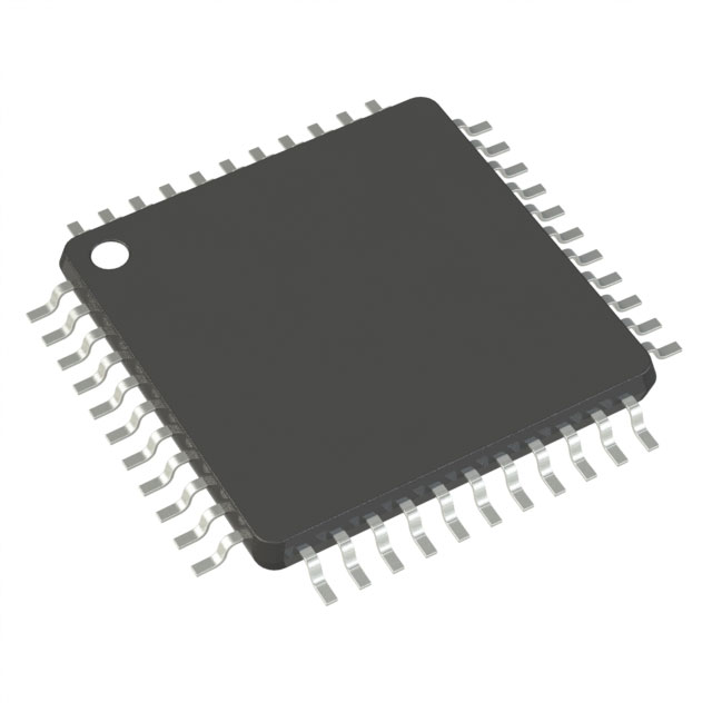
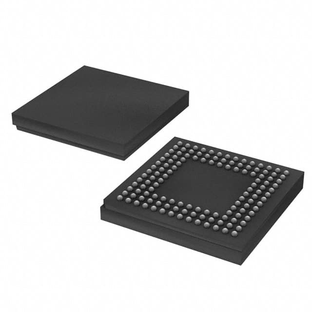
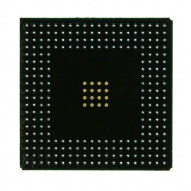
| 封裝/外殼 | 324-BBGA | |
| 可編程 | 未驗證 | |
| 供應商器件封裝 | 324-FBGA(23x23) | |
| 可編程類型 | 系統內可編程 | |
| 延遲時間 tpd(1) 最大值 | 9.2 ns | |
| 供電電壓 - 內部 | 1.7V ~ 1.9V | |
| 邏輯元件/塊數 | 32 | |
| 宏單元數 | 512 | |
| 柵極數 | 12000 | |
| I/O 數 | 270 | |
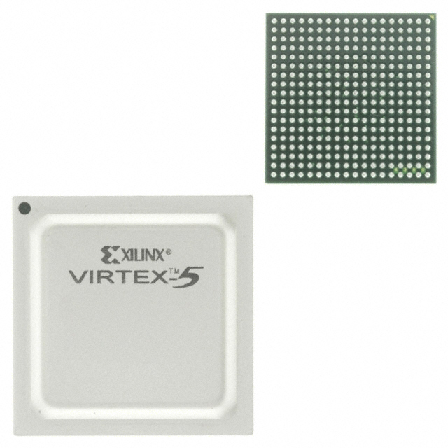
| 系列 | CoolRunner II | |
| 工作温度 | -40°C ~ 85°C(TA) | |
| 包裝 | 託盤 | |
| 安裝類型 | 表面貼裝型 | |
| 產品狀態 | 在售 |
部落格
 芯能王電子有限公司祝您感恩節快樂感谢您成为芯能王电子大家庭不可或缺的一员,祝您感恩节快乐!
 探索 Nvidia H200 在 AI 模型訓練方面的強大功能使用Nvidia的H200芯片探索AI训练的尖端可能性。解锁您的AI模型的最终潜力,并彻底改变您的工作。
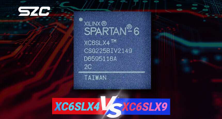 XC6SLX4 vs XC6SLX9:哪個更好?利用 XC6SLX4 和 XC6SLX9 FPGA 的潜力来增强性能和多功能性。
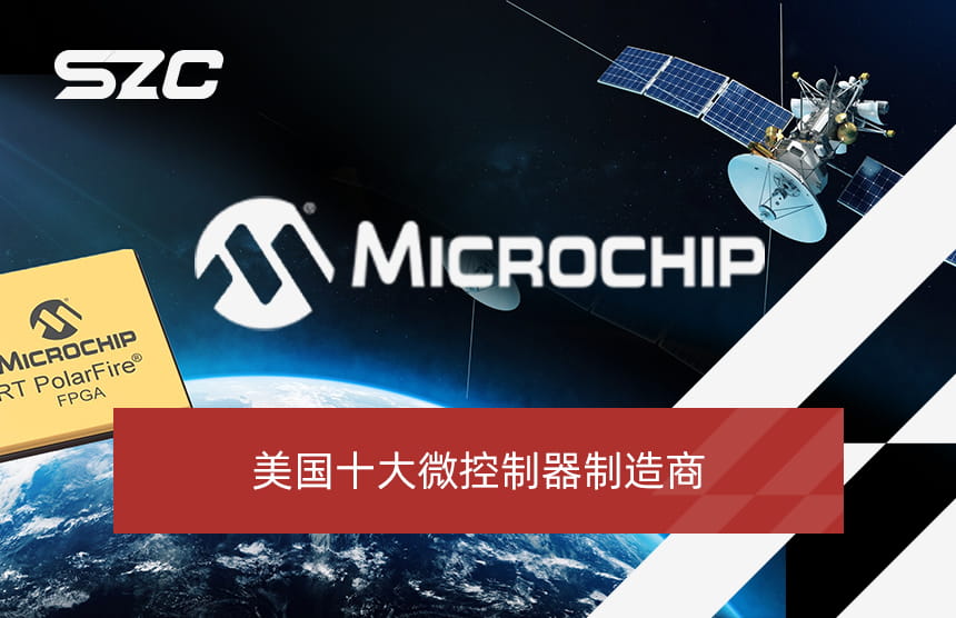 美國十大微控制器製造商本文章主要介绍美国前十微控制器制造商。
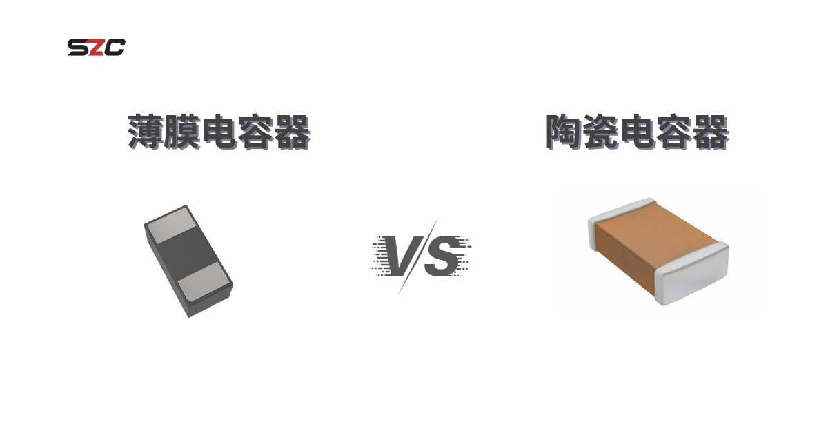 薄膜與陶瓷:選擇適合您的電容器当我们揭开薄膜和陶瓷电容器的神秘面纱时,探索电子元件的世界。在这个技术爱好者的指南中,系好安全带,通过电容电流进行迷人的旅程。

¥650.00
價格更新:一個月前
現貨供應:
500
AMD
AMD是全可編程FPGA、SoC、MPSoC和3D IC的領先提供商。AMD獨特地實現了軟件定義和硬件優化的應用-推動了雲計算,5G無線,嵌入式視覺和工業物聯網領域的行業進步。
查看所有産品從 AMD部落格
- 芯能王電子有限公司祝您感恩節快樂感谢您成为芯能王电子大家庭不可或缺的一员,祝您感恩节快乐!
- 探索 Nvidia H200 在 AI 模型訓練方面的強大功能使用Nvidia的H200芯片探索AI训练的尖端可能性。解锁您的AI模型的最终潜力,并彻底改变您的工作。
- XC6SLX4 vs XC6SLX9:哪個更好?利用 XC6SLX4 和 XC6SLX9 FPGA 的潜力来增强性能和多功能性。
- 美國十大微控制器製造商本文章主要介绍美国前十微控制器制造商。
- 薄膜與陶瓷:選擇適合您的電容器当我们揭开薄膜和陶瓷电容器的神秘面纱时,探索电子元件的世界。在这个技术爱好者的指南中,系好安全带,通过电容电流进行迷人的旅程。
熱門製造商
View all manufactures 更多


熱門產品
更多電子零件 更多XC2C512-10FGG324I
IC CPLD 512MC 9.2NS 324FBGA

XC2C128-7VQG100C
IC CPLD 128MC 7NS 100VQFP
XCR3256XL-10TQ144I
IC CPLD 256MC 9.1NS 144TQFP

XC2C384-10TQG144C
IC CPLD 384MC 9.2NS 144TQFP
XCR3064XL-10VQG44I
IC CPLD 64MC 9.1NS 44VQFP

XCR3032XL-10VQG44I
IC CPLD 32MC 9.1NS 44VQFP
XCR3064XL-6VQG100C
IC CPLD 64MC 5.5NS 100VQFP
XC2C128-7CPG132I
IC CPLD 128MC 7NS 132CSPBGA

XC95288XL-10TQ144I
IC CPLD 288MC 10NS 144TQFP
XC95288XL-10BG256I
IC CPLD 288MC 10NS 256BGA