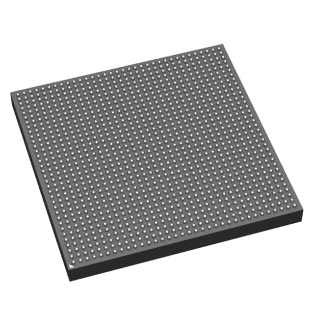
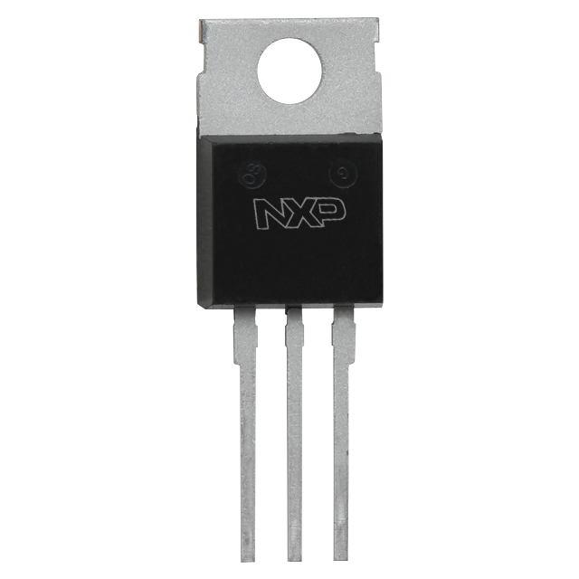
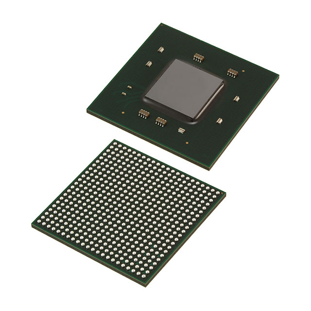
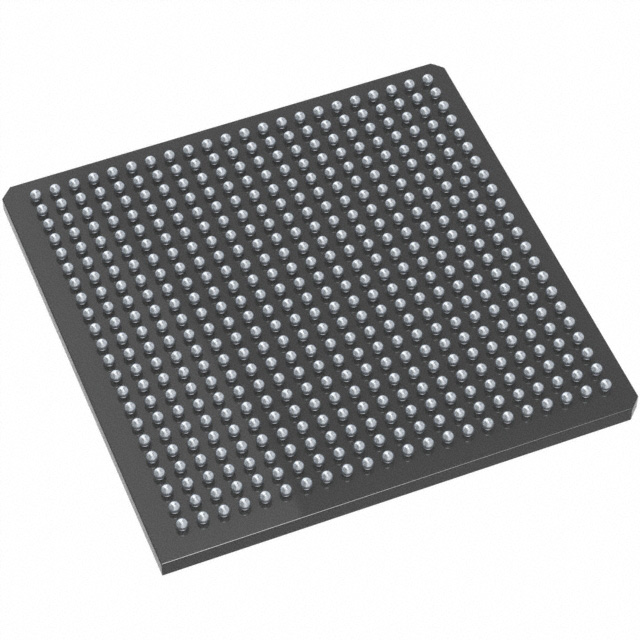
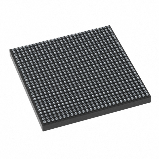
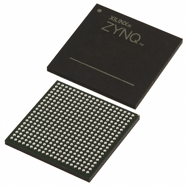
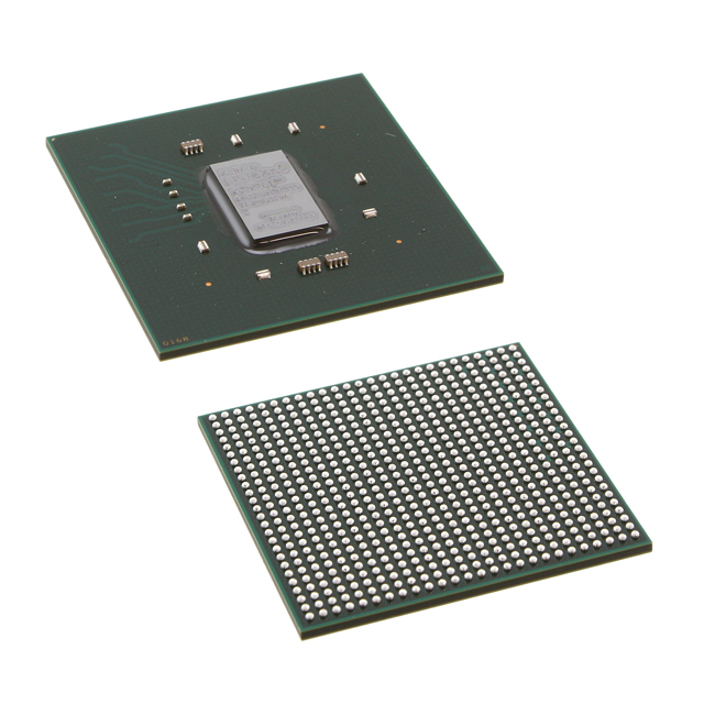
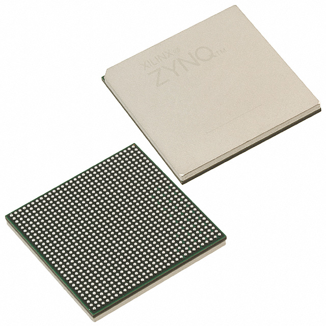
XCZU47DR-1FFVE1156I
對比
XCZU47DR-1FFVE1156I
IC ZUP RFSOC A53 FPGA 1156BGA


對比
¥23800.00
價格更新:一個月前
現貨供應:
4701


45
為45個國家的客戶提供服務
1000+
全球製造商
$140M
5年增長1.4億美元
50.0M+
5年內配送了5000萬個元件

AMD
AMD是全可編程FPGA、SoC、MPSoC和3D IC的領先提供商。AMD獨特地實現了軟件定義和硬件優化的應用-推動了雲計算,5G無線,嵌入式視覺和工業物聯網領域的行業進步。
查看所有産品從 AMD


The Zynq® UltraScale+™ RFSoC family integrates key subsystems for multiband, multi-mode cellular radios and cable infrastructure (DOCSIS) into an SoC platform that contains a feature-rich 64-bit quad-core Arm® Cortex™-A53 and dual-core Arm Cortex-R5 based processing system.
Combining the processing system with UltraScale™ architecture programmable logic and RF-ADCs, RF-DACs, and soft-decision FECs, the Zynq UltraScale+ RFSoC family is capable of implementing a complete software-defined radio including direct RF sampling data converters, enabling CPRI™ and gigabit Ethernet-to-RF on a single, highly programmable SoC.
Three generations of Zynq UltraScale+ RFSoCs integrate up to 16 channels of RF-ADCs and RF-DACs, all with excellent noise spectral density. The RF data converters also include power efficient digital down converters (DDCs) and digital up converters (DUCs) that include programmable interpolation and decimation, NCO, and complex mixer. The DDCs and DUCs can also support dual-band operation. See Table 1 for key features and sample rates.
Feature
RF Data Converter Subsystem Overview Most Zynq UltraScale+ RFSoCs include an RF data converter subsystem, which contains multiple radio frequency analog to digital converters (RF-ADCs) and multiple radio frequency digital to analog converters (RF-DACs). The high-precision, high-speed, power efficient RF-ADCs and RF-DACs can be individually configured for real data or can be configured in pairs for real and imaginary I/Q data.
Soft Decision Forward Error Correction (SD-FEC) Overview Some Zynq UltraScale+ RFSoCs include highly flexible soft-decision FEC blocks for decoding and encoding data as a means to control errors in data transmission over unreliable or noisy communication channels. The SD-FEC blocks support low-density parity check (LDPC) decode/encode and Turbo decode for use in 5G wireless, backhaul, DOCSIS, and LTE applications.
Processing System Overview Zynq UltraScale+ RFSoCs feature a quad-core Arm Cortex-A53 (APU) with a dual-core Arm Cortex-R5 (RPU) processing system (PS). To support the processors' functionality, a number of peripherals with dedicated functions are included in the PS. For interfacing to external memories for data or configuration storage, the PS includes a multi-protocol dynamic memory controller, a DMA controller, a NAND controller, an SD/eMMC controller and a Quad SPI controller. In addition to interfacing to external memories, the APU also includes a Level-1 (L1) and Level-2 (L2) cache hierarchy; the RPU includes an L1 cache and Tightly Coupled memory subsystem. Each has access to a 256KB on-chip memory. For high-speed interfacing, the PS includes 4 channels of transmit (TX) and receive (RX) pairs of transceivers, called PS-GTR transceivers, supporting data rates of up to 6.0Gb/s. These transceivers can interface to the high-speed peripheral blocks that support PCIe® at 5.0GT/s (Gen2) as a root complex or Endpoint in x1, x2, or x4 configurations; Serial-ATA (SATA) at 1.5Gb/s, 3.0Gb/s, or 6.0Gb/s data rates; and up to two lanes of DisplayPort at 1.62Gb/s, 2.7Gb/s, or 5.4Gb/s data rates. The PS-GTR transceivers can also interface to components over USB 3.0 and Serial Gigabit Media Independent Interface (SGMII). For general connectivity, the PS includes: a pair of USB 2.0 controllers, which can be configured as host, device, or On-The-Go (OTG); an I2C controller; a UART; and a CAN2.0B controller that conforms to ISO11898-1. There are also four triple speed Ethernet MACs and 128 bits of GPIO, of which 78 bits are available through the MIO and 96 through the EMIO. High-bandwidth connectivity based on the Arm AMBA® AXI4 protocol connects the processing units with the peripherals and provides interface between the PS and the programmable logic (PL).
I/O, Transceiver, PCIe, 100G Ethernet, and 150G Interlaken Data is transported on and off chip through a combination of the high-performance parallel SelectIO™ interface and high-speed serial transceiver connectivity. I/O blocks provide support for cutting-edge memory interface and network protocols through flexible I/O standard and voltage support. The serial transceivers in the UltraScale architecture-based devices transfer data up to 28.21Gb/s, enabling 25G+ backplane designs with dramatically lower power per bit than previous generation transceivers. All transceivers, except the PS-GTR, support the required data rates for 8.0GT/s (Gen3) and 16.0GT/s (Gen4) for PCIe. The integrated blocks for PCIe can be configured as either Endpoint or Root Port, supporting a variety of link widths and speeds depending on the targeted device speed grade and package. Integrated blocks for 150Gb/s Interlaken and 100Gb/s Ethernet (100G MAC/PCS) extend the capabilities of UltraScale™ devices, enabling simple, reliable support for Nx100G switch and bridge applications.
Clocks and Memory Interfaces Zynq UltraScale+ RFSoCs contain powerful clock management circuitry, including clock synthesis, buffering, and routing components that together provide a highly capable framework to meet design requirements. The clock network allows for extremely flexible distribution of clocks to minimize the skew, power consumption, and delay associated with clock signals. The clock management technology is tightly integrated with dedicated memory interface circuitry to enable support for high-performance external memories, including DDR4. In addition to parallel memory interfaces, Zynq UltraScale+ RFSoCs support serial memories, such as hybrid memory cube (HMC).
Routing, Logic, Storage, and Signal Processing Configurable logic blocks (CLBs) containing 6-input look-up tables (LUTs) and flip-flops, DSP slices with 27x18 multipliers, 36Kb block RAMs with built-in FIFO and ECC support, and 4Kx72 UltraRAM blocks are all connected with an abundance of high-performance, low-latency interconnect. In addition to logical functions, the CLB provides shift register, multiplexer, and carry logic functionality as well as the ability to configure the LUTs as distributed memory to complement the highly capable and configurable block RAMs. The DSP slice, with its 96-bit-wide XOR functionality, 27-bit pre-adder, and 30-bit A input, performs numerous independent functions including multiply accumulate, multiply add, and pattern detect.
Configuration, Encryption, and System Monitoring Zynq UltraScale+ RFSoCs are booted via the configuration security unit (CSU), which supports secure boot via the 256-bit AES-GCM and SHA/384 blocks. The cryptographic engines in the CSU can be used in the RFSoC after boot for user encryption. The System Monitor enables the monitoring of the physical environment via on-chip temperature and supply sensors and can also monitor up to 17 external analog inputs.


產品屬性
| 類型 | 描述 | 全選 |
|---|---|---|
| 核心處理器 | 帶 CoreSight™ 的四核 ARM® Cortex®-A53 MPCore™,帶 CoreSight™ 的雙核 ARM®Cortex™-R5 | |
| RAM 大小 | 256KB | |
| 外設 | DMA,WDT | |
| 連接能力 | CANbus,EBI/EMI,以太網,I²C,MMC/SD/SDIO,SPI,UART/USART,USB OTG | |
| 速度 | 500MHz,1.2GHz | |
| 主要屬性 | Zynq®UltraScale+™ FPGA,930K+ 邏輯單元 | |
| 系列 | Zynq® UltraScale+™ RFSoC | |
| 工作温度 | -40°C ~ 100°C(TJ) | |
| 包裝 | 託盤 | |
| 封裝/外殼 | 1156-BBGA,FCBGA | |
| 產品狀態 | 在售 | |
| 供應商器件封裝 | 1156-FCBGA(35x35) | |
| 架構 | MCU,FPGA |
部落格
 芯能王電子有限公司祝您感恩節快樂感谢您成为芯能王电子大家庭不可或缺的一员,祝您感恩节快乐!
 探索 Nvidia H200 在 AI 模型訓練方面的強大功能使用Nvidia的H200芯片探索AI训练的尖端可能性。解锁您的AI模型的最终潜力,并彻底改变您的工作。
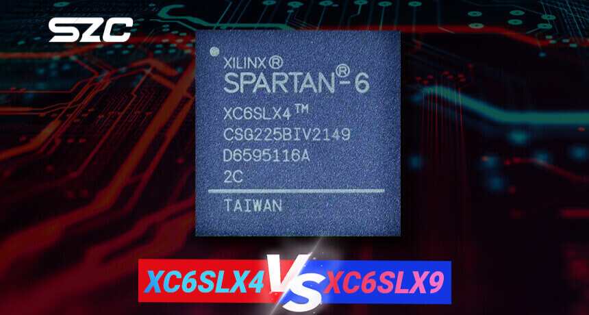 XC6SLX4 vs XC6SLX9:哪個更好?利用 XC6SLX4 和 XC6SLX9 FPGA 的潜力来增强性能和多功能性。
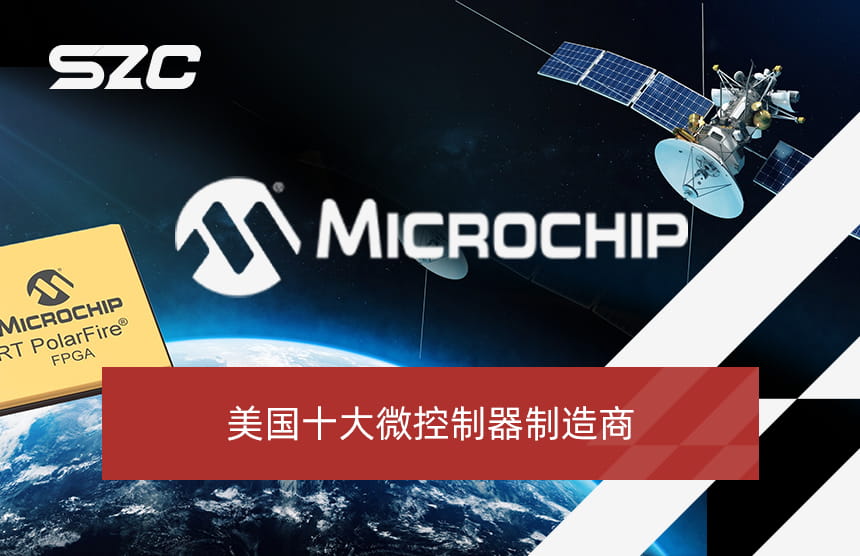 美國十大微控制器製造商本文章主要介绍美国前十微控制器制造商。
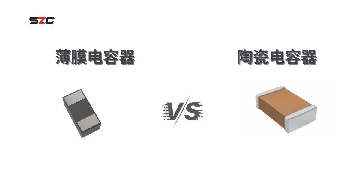 薄膜與陶瓷:選擇適合您的電容器当我们揭开薄膜和陶瓷电容器的神秘面纱时,探索电子元件的世界。在这个技术爱好者的指南中,系好安全带,通过电容电流进行迷人的旅程。

¥23800.00
價格更新:一個月前
現貨供應:
4701
AMD
AMD是全可編程FPGA、SoC、MPSoC和3D IC的領先提供商。AMD獨特地實現了軟件定義和硬件優化的應用-推動了雲計算,5G無線,嵌入式視覺和工業物聯網領域的行業進步。
查看所有産品從 AMD部落格
- 芯能王電子有限公司祝您感恩節快樂感谢您成为芯能王电子大家庭不可或缺的一员,祝您感恩节快乐!
- 探索 Nvidia H200 在 AI 模型訓練方面的強大功能使用Nvidia的H200芯片探索AI训练的尖端可能性。解锁您的AI模型的最终潜力,并彻底改变您的工作。
- XC6SLX4 vs XC6SLX9:哪個更好?利用 XC6SLX4 和 XC6SLX9 FPGA 的潜力来增强性能和多功能性。
- 美國十大微控制器製造商本文章主要介绍美国前十微控制器制造商。
- 薄膜與陶瓷:選擇適合您的電容器当我们揭开薄膜和陶瓷电容器的神秘面纱时,探索电子元件的世界。在这个技术爱好者的指南中,系好安全带,通过电容电流进行迷人的旅程。
熱門製造商
View all manufactures 更多


熱門產品
更多電子零件 更多XCZU47DR-1FFVE1156I
IC ZUP RFSOC A53 FPGA 1156BGA
XC7Z030-1FBG484C
IC SOC CORTEX-A9 667MHZ 484FCBGA
XCZU2EG-L1SBVA484I
IC SOC CORTEX-A53 484FCBGA
XCZU1CG-2SBVA484I
IC ZUP MPSOC CG A53 FPGA 484BGA
XAZU1EG-1SFVC784I
IC ZUP MPSOC A53 FPGA Q 784BGA
XAZU1EG-1SBVA484Q
IC ZUP MPSOC A53 FPGA Q 484BGA
XC7Z010-1CLG400I
IC SOC CORTEX-A9 667MHZ 400BGA
XC7Z020-1CLG400C
IC SOC CORTEX-A9 667MHZ 400BGA
XC7Z030-1FBG676C
IC SOC CORTEX-A9 667MHZ 676FCBGA
XC7Z035-2FFG900I
IC SOC CORTEX-A9 800MHZ 900FCBGA