


¥40.00
價格更新:一個月前
現貨供應:
6500


45
為45個國家的客戶提供服務
1000+
全球製造商
$140M
5年增長1.4億美元
50.0M+
5年內配送了5000萬個元件

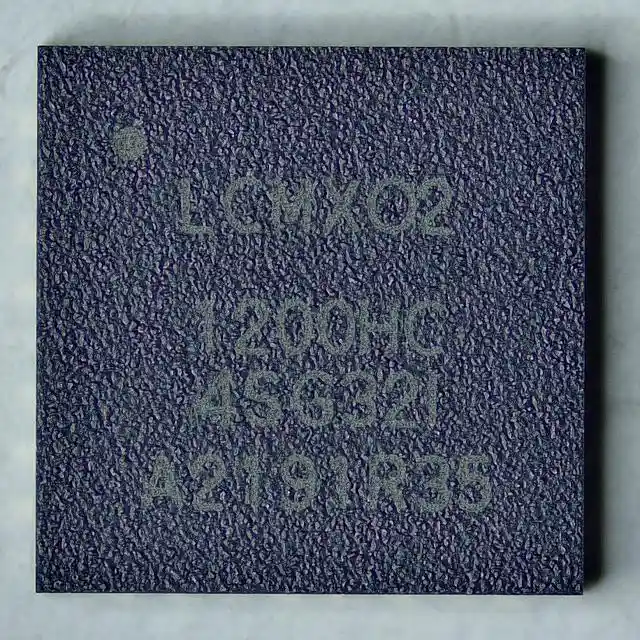
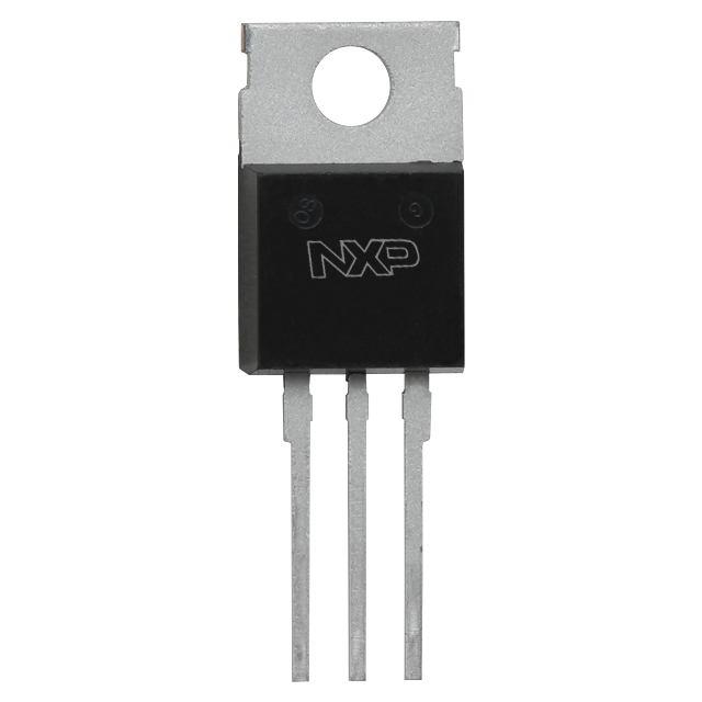
Lattice Semiconductor Corporation
Lattice Semiconductor 是低功耗可編程的領導者。 在不斷增長的通信、計算、工業、汽車和消費市場中,他們通過網絡解決客户問題,從邊緣到雲端。 他們的技術、長期合作關係以及對世界級支持的承諾讓他們的客户能夠快速、輕鬆地釋放他們的創新,以創造一個智能、安全和互聯的世界。
查看所有産品從 Lattice Semiconductor Corporation


The MachXO2 family of ultra low power, instant-on, non-volatile PLDs has six devices with densities ranging from 256 to 6864 Look-Up Tables (LUTs). In addition to LUT-based, low-cost programmable logic these devices feature Embedded Block RAM (EBR), Distributed RAM, User Flash Memory (UFM), Phase Locked Loops (PLLs), preengineered source synchronous I/O support, advanced configuration support including dual-boot capability and hardened versions of commonly used functions such as SPI controller, I2 C controller and timer/counter. These features allow these devices to be used in low cost, high volume consumer and system applications.
The MachXO2 devices are designed on a 65nm non-volatile low power process. The device architecture has several features such as programmable low swing differential I/Os and the ability to turn off I/O banks, on-chip PLLs and oscillators dynamically. These features help manage static and dynamic power consumption resulting in low static power for all members of the family.
The MachXO2 devices are available in two versions – ultra low power (ZE) and high performance (HC and HE) devices. The ultra low power devices are offered in three speed grades -1, -2 and -3, with -3 being the fastest. Similarly, the high-performance devices are offered in three speed grades: -4, -5 and -6, with -6 being the fastest. HC devices have an internal linear voltage regulator which supports external VCC supply voltages of 3.3V or 2.5V. ZE and HE devices only accept 1.2V as the external VCC supply voltage. With the exception of power supply voltage all three types of devices (ZE, HC and HE) are functionally compatible and pin compatible with each other.
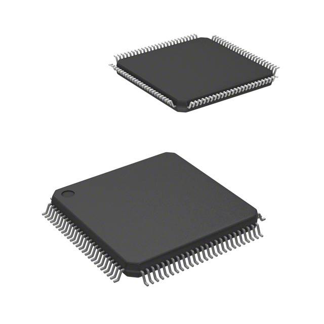
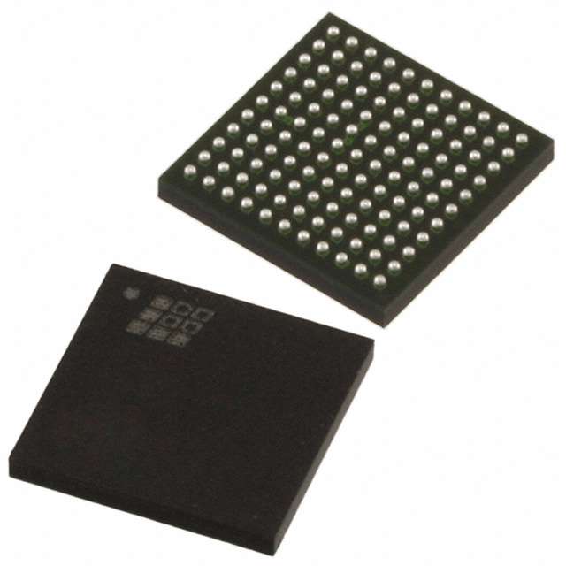
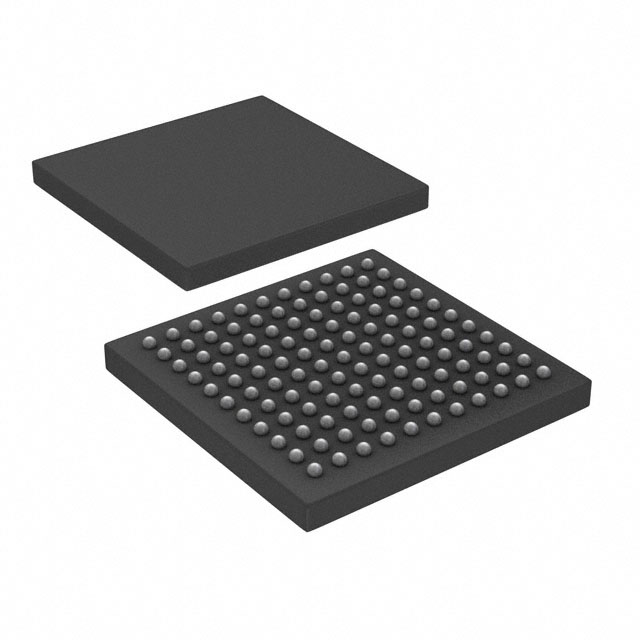
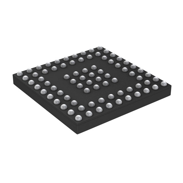
The MachXO2 PLDs are available in a broad range of advanced halogen-free packages ranging from the space saving 2.5x2.5 mm WLCSP to the 23x23 mm fpBGA. MachXO2 devices support density migration within the same package. Table 1-1 shows the LUT densities, package and I/O options, along with other key parameters.
The pre-engineered source synchronous logic implemented in the MachXO2 device family supports a broad range of interface standards, including LPDDR, DDR, DDR2 and 7:1 gearing for display I/Os.
The MachXO2 devices offer enhanced I/O features such as drive strength control, slew rate control, PCI compatibility, bus-keeper latches, pull-up resistors, pull-down resistors, open drain outputs and hot socketing. Pull-up, pulldown and bus-keeper features are controllable on a “per-pin” basis.
A user-programmable internal oscillator is included in MachXO2 devices. The clock output from this oscillator may be divided by the timer/counter for use as clock input in functions such as LED control, key-board scanner and similar state machines.
The MachXO2 devices also provide flexible, reliable and secure configuration from on-chip Flash memory. These devices can also configure themselves from external SPI Flash or be configured by an external master through the JTAG test access port or through the I2 C port. Additionally, MachXO2 devices support dual-boot capability (using external Flash memory) and remote field upgrade (TransFR) capability.
Feature
Flexible Logic Architecture
• Six devices with 256 to 6864 LUT4s and 19 to 335 I/Os
Ultra Low Power Devices
• Advanced 65 nm low power process
• As low as 19 µW standby power
• Programmable low swing differential I/Os
• Stand-by mode and other power saving options
Embedded and Distributed Memory
• Up to 240 Kbits sysMEM™ Embedded Block RAM
• Up to 54 Kbits Distributed RAM
• Dedicated FIFO control logic
On-Chip User Flash Memory
• Up to 256 Kbits of User Flash Memory
• 100,000 write cycles
• Accessible through WISHBONE, SPI, I2 C and JTAG interfaces
• Can be used as soft processor PROM or as Flash memory
Pre-Engineered Source Synchronous I/O
• DDR registers in I/O cells
• Dedicated gearing logic
• 7:1 Gearing for Display I/Os
• Generic DDR, DDRX2, DDRX4
• Dedicated DDR/DDR2/LPDDR memory with DQS support
High Performance, Flexible I/O Buffer
• Programmable sysIO™ buffer supports wide range of interfaces:
– LVCMOS 3.3/2.5/1.8/1.5/1.2
– LVTTL
– PCI
– LVDS, Bus-LVDS, MLVDS, RSDS, LVPECL
– SSTL 25/18
– HSTL 18
– Schmitt trigger inputs, up to 0.5V hysteresis
• I/Os support hot socketing
• On-chip differential termination
• Programmable pull-up or pull-down mode
Flexible On-Chip Clocking
• Eight primary clocks
• Up to two edge clocks for high-speed I/O interfaces (top and bottom sides only)
• Up to two analog PLLs per device with fractional-n frequency synthesis – Wide input frequency range (10 MHz to 400 MHz)
Non-volatile, Infinitely Reconfigurable
• Instant-on – powers up in microseconds
• Single-chip, secure solution
• Programmable through JTAG, SPI or I2 C
• Supports background programming of non-volatile memory
• Optional dual boot with external SPI memory
TransFR™ Reconfiguration
• In-field logic update while system operates
Enhanced System Level Support
• On-chip hardened functions: SPI, I2 C, timer/ counter
• On-chip oscillator with 5.5% accuracy
• Unique TraceID for system tracking
• One Time Programmable (OTP) mode
• Single power supply with extended operating range
• IEEE Standard 1149.1 boundary scan
• IEEE 1532 compliant in-system programming
Broad Range of Package Options
• TQFP, WLCSP, ucBGA, csBGA, caBGA, ftBGA, fpBGA, QFN package options
• Small footprint package options – As small as 2.5x2.5mm
• Density migration supported
• Advanced halogen-free packaging


相關產品
| 製造商零件編號 | 價格(¥) | 現有數量 | |
|---|---|---|---|
 ICE5LP2K-SG48ITRIC FPGA 39 I/O 48QFN | 150.00 |
1845
市場 | |
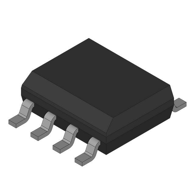
 LCMXO2-1200HC-4SG32CIC FPGA 21 I/O 32QFNS | 33.00 |
4900
市場 |
產品屬性
| 類型 | 描述 | 全選 |
|---|---|---|
| 系列 | MachXO2 | |
| 包裝 | 託盤 | |
| 產品狀態 | 在售 | |
| 可編程 | 未驗證 | |
| LAB/CLB 數 | 160 | |
| 邏輯元件/單元數 | 1280 | |
| 總 RAM 位數 | 65536 | |
| I/O 數 | 21 | |
| 電壓 - 供電 | 2.375V ~ 3.465V | |
| 安裝類型 | 表面貼裝型 | |
| 工作温度 | -40°C ~ 100°C(TJ) | |
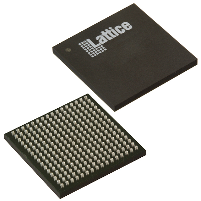
| 封裝/外殼 | 32-UFQFN 裸露焊盤 | |
| 供應商器件封裝 | 32-QFN(5x5) |
部落格
 芯能王電子有限公司祝您感恩節快樂感谢您成为芯能王电子大家庭不可或缺的一员,祝您感恩节快乐!
 探索 Nvidia H200 在 AI 模型訓練方面的強大功能使用Nvidia的H200芯片探索AI训练的尖端可能性。解锁您的AI模型的最终潜力,并彻底改变您的工作。
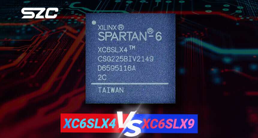 XC6SLX4 vs XC6SLX9:哪個更好?利用 XC6SLX4 和 XC6SLX9 FPGA 的潜力来增强性能和多功能性。
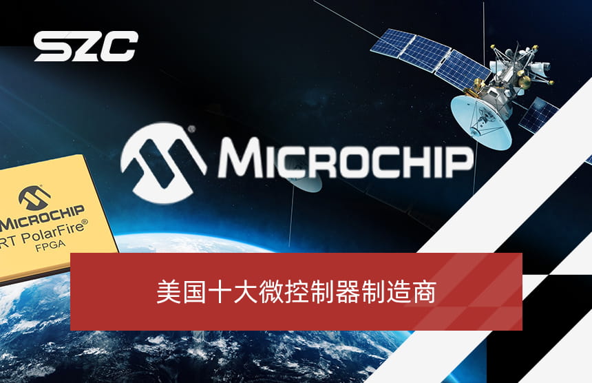 美國十大微控制器製造商本文章主要介绍美国前十微控制器制造商。
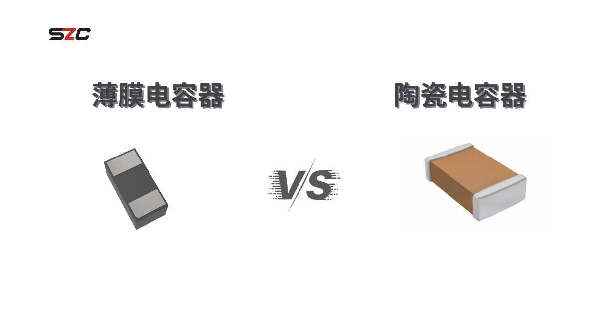 薄膜與陶瓷:選擇適合您的電容器当我们揭开薄膜和陶瓷电容器的神秘面纱时,探索电子元件的世界。在这个技术爱好者的指南中,系好安全带,通过电容电流进行迷人的旅程。

¥40.00
價格更新:一個月前
現貨供應:
6500
Lattice Semiconductor Corporation
Lattice Semiconductor 是低功耗可編程的領導者。 在不斷增長的通信、計算、工業、汽車和消費市場中,他們通過網絡解決客户問題,從邊緣到雲端。 他們的技術、長期合作關係以及對世界級支持的承諾讓他們的客户能夠快速、輕鬆地釋放他們的創新,以創造一個智能、安全和互聯的世界。
查看所有産品從 Lattice Semiconductor Corporation部落格
- 芯能王電子有限公司祝您感恩節快樂感谢您成为芯能王电子大家庭不可或缺的一员,祝您感恩节快乐!
- 探索 Nvidia H200 在 AI 模型訓練方面的強大功能使用Nvidia的H200芯片探索AI训练的尖端可能性。解锁您的AI模型的最终潜力,并彻底改变您的工作。
- XC6SLX4 vs XC6SLX9:哪個更好?利用 XC6SLX4 和 XC6SLX9 FPGA 的潜力来增强性能和多功能性。
- 美國十大微控制器製造商本文章主要介绍美国前十微控制器制造商。
- 薄膜與陶瓷:選擇適合您的電容器当我们揭开薄膜和陶瓷电容器的神秘面纱时,探索电子元件的世界。在这个技术爱好者的指南中,系好安全带,通过电容电流进行迷人的旅程。
熱門製造商
View all manufactures 更多


熱門產品
更多電子零件 更多LCMXO2-1200HC-4SG32I
IC FPGA 21 I/O 32QFNS
ICE40LP384-SG32
IC FPGA 21 I/O 32QFN

LCMXO2-256HC-5SG32C
IC FPGA 21 I/O 32QFNS
ICE40HX1K-VQ100
IC FPGA 72 I/O 100TQFP
ICE40LP1K-CB121
IC FPGA 92 I/O 121CSBGA
ICE40HX4K-BG121
IC FPGA 93 I/O 121CABGA
LCMXO2-1200HC-6TG100C
IC FPGA 79 I/O 100TQFP
LIF-MD6000-6JMG80I
IC FPGA 37 I/O 80CTFBGA
LIA-MD6000-6JMG80E
IC FPGA 37 I/O 80CTFBGA
LCMXO3LF-6900E-6MG256C
IC FPGA 206 I/O 256CSFBGA