


¥5.36
價格更新:一個月前
現貨供應:
4534


45
為45個國家的客戶提供服務
1000+
全球製造商
$140M
5年增長1.4億美元
50.0M+
5年內配送了5000萬個元件

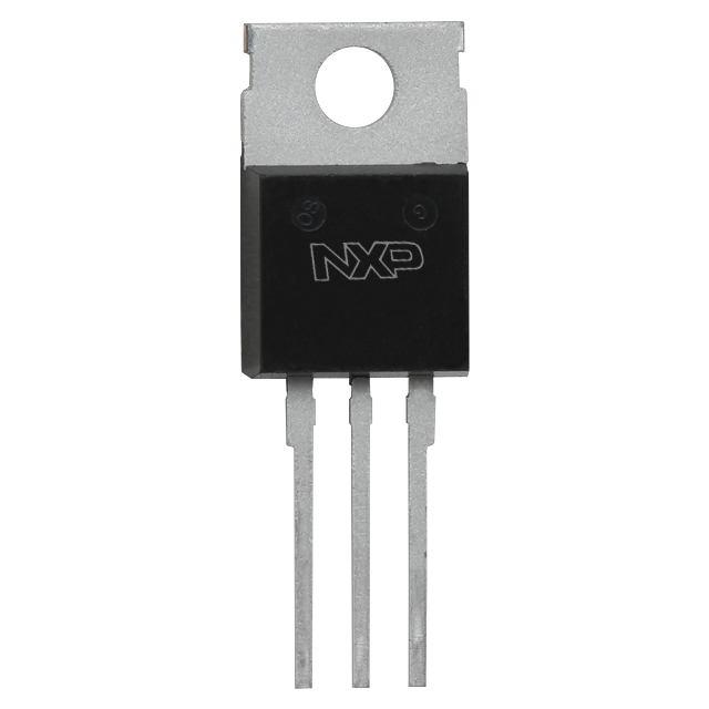
Texas Instruments
德州儀器 (TI) 是一家開發模擬 IC 和嵌入式處理器的全球半導體設計和製造公司。 通過聘用世界上最聰明的人才,TI 創造了塑造技術未來的創新。 今天,TI 正在幫助超過 100,000 家客户改變未來。
查看所有産品從 Texas Instruments


Data sheet acquired from Harris Semiconductor
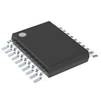
DescriptionThe device is useful in a wide variety of shifting, counting and storage applications. It performs serial, parallel, serial to parallel, or parallel to serial data transfers at very high speeds.
The two modes of operation, shift right (Q0-Q1) and parallel load, are controlled by the state of the Parallel Enable (PE)\ input. Serial data enters the first flip-flop (Q0) via the J and K\ inputs when the PE\ input is high, and is shifted one bit in the direction Q0-Q1-Q2-Q3 following each Low to High clock transition. The J and K\ inputs provide the flexibility of the JK-type input for special applications and by tying the two pins together, the simple D-type input for general applications. The device appears as four common-clocked D flip-flops when the PE\ input is Low. After the Low to High clock transition, data on the parallel inputs (D0-D3) is transferred to the respective Q0-Q3 outputs. Shift left operation (Q3-Q2) can be achieved by tying the Qn outputs to the Dn-1 inputs and holding the PE\ input low.
All parallel and serial data transfers are synchronous, occurring after each Low to High clock transition. The ’HC195 series utilizes edge triggering; therefore, there is no restriction on the activity of the J, K\, Pn and PE\ inputs for logic operations, other than set-up and hold time requirements. A Low on the asynchronous Master Reset (MR)\ input sets all Q outputs Low, independent of any other input condition.
Feature
- Asynchronous Master Reset
- J, K\,(D) Inputs to First Stage
- Fully Synchronous Serial or Parallel Data Transfer
- Shift Right and Parallel Load Capability
- Complementary Output From Last Stage
- Buffered Inputs
- Typical fMAX = 50MHz at VCC = 5V, CL = 15pF, TA = 25°C
- Fanout (Over Temperature Range)
- Standard Outputs . . . . 10 LSTTL Loads
- Bus Driver Outputs . . . . 15 LSTTL Loads
- Wide Operating Temperature Range . . . –55°C to 125°C
- Balanced Propagation Delay and Transition Times
- Significant Power Reduction Compared to LSTTL Logic ICs
- HC Types
- 2V to 6V Operation
- High Noise Immunity: NIL = 30%, NIH = 30%of VCC at VCC = 5V
Data sheet acquired from Harris Semiconductor
DescriptionThe device is useful in a wide variety of shifting, counting and storage applications. It performs serial, parallel, serial to parallel, or parallel to serial data transfers at very high speeds.
The two modes of operation, shift right (Q0-Q1) and parallel load, are controlled by the state of the Parallel Enable (PE)\ input. Serial data enters the first flip-flop (Q0) via the J and K\ inputs when the PE\ input is high, and is shifted one bit in the direction Q0-Q1-Q2-Q3 following each Low to High clock transition. The J and K\ inputs provide the flexibility of the JK-type input for special applications and by tying the two pins together, the simple D-type input for general applications. The device appears as four common-clocked D flip-flops when the PE\ input is Low. After the Low to High clock transition, data on the parallel inputs (D0-D3) is transferred to the respective Q0-Q3 outputs. Shift left operation (Q3-Q2) can be achieved by tying the Qn outputs to the Dn-1 inputs and holding the PE\ input low.
All parallel and serial data transfers are synchronous, occurring after each Low to High clock transition. The ’HC195 series utilizes edge triggering; therefore, there is no restriction on the activity of the J, K\, Pn and PE\ inputs for logic operations, other than set-up and hold time requirements. A Low on the asynchronous Master Reset (MR)\ input sets all Q outputs Low, independent of any other input condition.


產品屬性
| 類型 | 描述 | 全選 |
|---|---|---|
| 功能 | 通用 | |
| 每個元件位數 | 4 | |
| 輸出類型 | 補充型 | |
| 邏輯類型 | 雙向寄存器 | |
| 產品狀態 | 在售 | |
| 包裝 | 卷帶(TR) | |
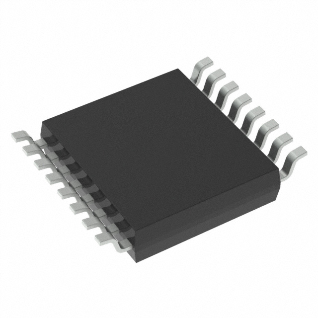
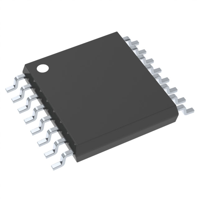
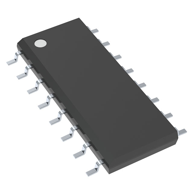
| 供應商器件封裝 | 16-TSSOP | |
| 系列 | 74HC | |
| 封裝/外殼 | 16-TSSOP(0.173",4.40mm 寬) | |
| 安裝類型 | 表面貼裝型 | |
| 工作温度 | -55°C ~ 125°C | |
| 電壓 - 供電 | 2V ~ 6V | |
| 元件數 | 1 |
部落格
 芯能王電子有限公司祝您感恩節快樂感谢您成为芯能王电子大家庭不可或缺的一员,祝您感恩节快乐!
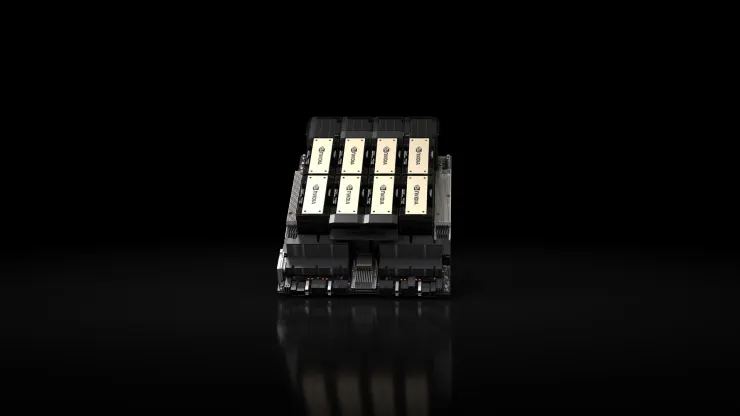 探索 Nvidia H200 在 AI 模型訓練方面的強大功能使用Nvidia的H200芯片探索AI训练的尖端可能性。解锁您的AI模型的最终潜力,并彻底改变您的工作。
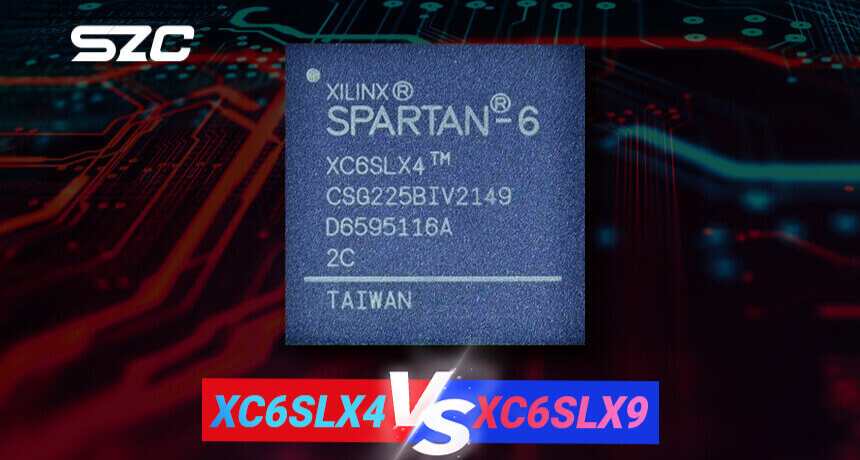 XC6SLX4 vs XC6SLX9:哪個更好?利用 XC6SLX4 和 XC6SLX9 FPGA 的潜力来增强性能和多功能性。
 美國十大微控制器製造商本文章主要介绍美国前十微控制器制造商。
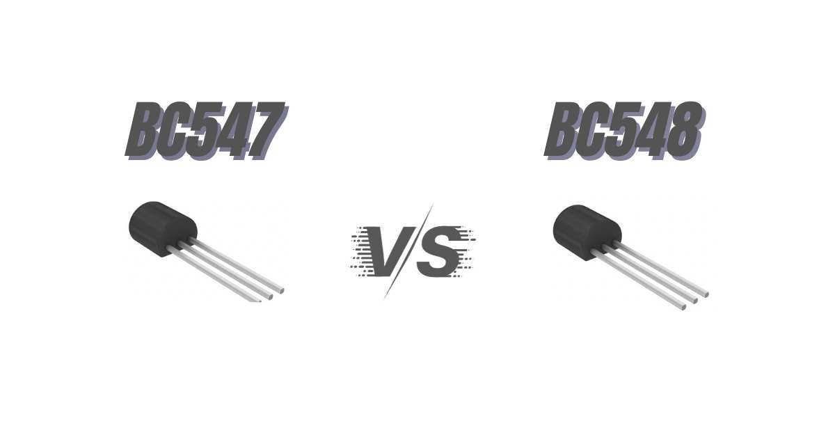
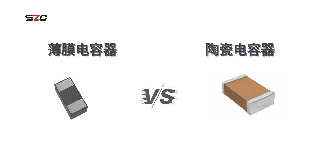 薄膜與陶瓷:選擇適合您的電容器当我们揭开薄膜和陶瓷电容器的神秘面纱时,探索电子元件的世界。在这个技术爱好者的指南中,系好安全带,通过电容电流进行迷人的旅程。


¥5.36
價格更新:一個月前
現貨供應:
4534
Texas Instruments
德州儀器 (TI) 是一家開發模擬 IC 和嵌入式處理器的全球半導體設計和製造公司。 通過聘用世界上最聰明的人才,TI 創造了塑造技術未來的創新。 今天,TI 正在幫助超過 100,000 家客户改變未來。
查看所有産品從 Texas Instruments部落格
- 芯能王電子有限公司祝您感恩節快樂感谢您成为芯能王电子大家庭不可或缺的一员,祝您感恩节快乐!
- 探索 Nvidia H200 在 AI 模型訓練方面的強大功能使用Nvidia的H200芯片探索AI训练的尖端可能性。解锁您的AI模型的最终潜力,并彻底改变您的工作。
- XC6SLX4 vs XC6SLX9:哪個更好?利用 XC6SLX4 和 XC6SLX9 FPGA 的潜力来增强性能和多功能性。
- 美國十大微控制器製造商本文章主要介绍美国前十微控制器制造商。
- 薄膜與陶瓷:選擇適合您的電容器当我们揭开薄膜和陶瓷电容器的神秘面纱时,探索电子元件的世界。在这个技术爱好者的指南中,系好安全带,通过电容电流进行迷人的旅程。
熱門製造商
View all manufactures 更多


熱門產品
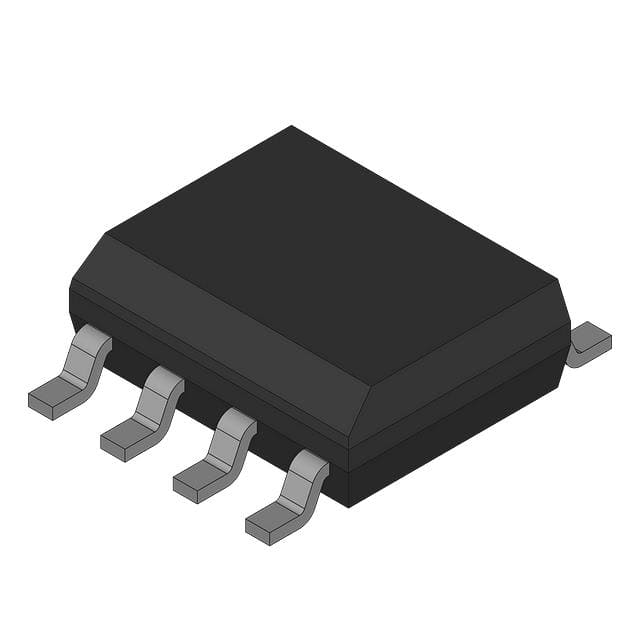
更多電子零件 更多CD74HC195PWR
IC 4-BIT ACCESS REGISTER 16TSSOP
SN74LS299N
SHIFT REGISTER SINGLE 8-BIT
SN74HC165PWR
IC 8-BIT SHIFT REGISTER 16-TSSOP
TPIC6595N
IC PWR 8-BIT SHIFT REGIS 20-DIP
SN74HCS166PWR
IC SHIFT REGISTER 8 BIT 16TSSOP
SN74HC595PWR
IC 8BIT SHIFT REGISTER 16-TSSOP
SN74HC166DR
IC 8BIT SERIAL SHIFT REG 16-SOIC
CD74HCT165M96
IC 8BIT SHIFT REGISTER HS 16SOIC

SN74HC166PWR
IC SHIFT REGISTER 8BIT 16-TSSOP
SN74LV164ADR
IC REGISTER PAR-OUT 8BIT 14-SOIC