


45
為45個國家的客戶提供服務
1000+
全球製造商
$140M
5年增長1.4億美元
50.0M+
5年內配送了5000萬個元件
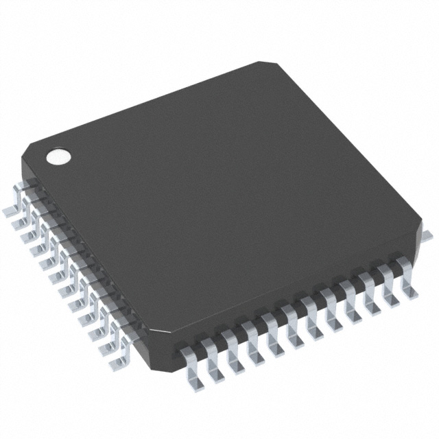
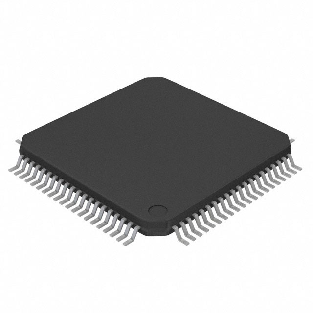
The TL16C2550PFBR is a dual universal asynchronous receiver and transmitter (UART). It incorporates the functionality of two TL16C550D UARTs, each UART having its own register set and FIFOs. The two UARTs share only the data bus interface and clock source, otherwise they operate independently. Another name for the uart function is Asynchronous Communications Element (ACE), and these terms will be used interchangeably. The bulk of this document describes the behavior of each ACE, with the understanding that two such devices are incorporated into the TL16C2550.
Each ACE is a speed and voltage range upgrade of the TL16C550C, which in turn is a functional upgrade of the TL16C450. Functionally equivalent to the TL16C450 on power up or reset (single character or TL16C450 mode), each ACE can be placed in an alternate FIFO mode. This relieves the CPU of excessive software overhead by buffering received and to be transmitted characters. Each receiver and transmitter store up to 16 bytes in their respective FIFOs, with the receive FIFO including three additional bits per byte for error status. In the FIFO mode, a selectable autoflow control feature can significantly reduce software overload and increase system efficiency by automatically controlling serial data flow using handshakes between the RXRDY output that can be used to interface to a DMA controller.
Feature
- Programmable Auto-RTS and Auto-CTS
- In Auto-CTS Mode, CTS Controls Transmitter
- In Auto-RTS Mode, RCV FIFO Contents, and Threshold Control RTS
- Serial and Modem Control Outputs Drive a RJ11 Cable Directly When Equipment Is on the Same Power Drop
- Capable of Running With All Existing TL16C450 Software
- After Reset, All Registers Are Identical to the TL16C450 Register Set
- Up to 24-MHz Clock Rate for up to 1.5-Mbaud Operation With VCC = 5 V
- Up to 20-MHz Clock Rate for up to 1.25-Mbaud Operation With VCC = 3.3 V
- Up to 16-MHz Clock Rate for up to 1-Mbaud Operation With VCC = 2.5 V
- Up to 10-MHz Clock Rate for up to 625-kbaud Operation With VCC = 1.8 V
- In the TL16C450 Mode, Hold and Shift Registers Eliminate the Need for Precise Synchronization Between the CPU and Serial Data
- Programmable Baud Rate Generator Allows Division of Any Input Reference Clock by 1 to (2 16 -1) and Generates an Internal 16 × Clock
- Standard Asynchronous Communication Bits (Start, Stop, and Parity) Added to or Deleted From the Serial Data Stream
- 5-V, 3.3-V, 2.5-V, and 1.8-V Operation
- Independent Receiver Clock Input
- Transmit, Receive, Line Status, and Data Set Interrupts Independently Controlled
- Fully Programmable Serial Interface Characteristics:
- 5-, 6-, 7-, or 8-Bit Characters
- Even-, Odd-, or No-Parity Bit Generation and Detection
- 1-, 1 1/2-, or 2-Stop Bit Generation
- Baud Generation (DC to 1 Mbit/s)
- False-Start Bit Detection
- Complete Status Reporting Capabilities
- 3-State Output TTL Drive Capabilities for Bidirectional Data Bus and Control Bus
- Line Break Generation and Detection Internal Diagnostic Capabilities:
- Loopback Controls for Communications Link Fault Isolation
- Break, Parity, Overrun, and Framing Error Simulation
- Fully Prioritized Interrupt System Controls
- Modem Control Functions (CTS, RTS, DSR, DTR, RI, and DCD)
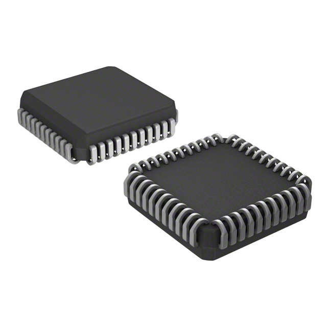
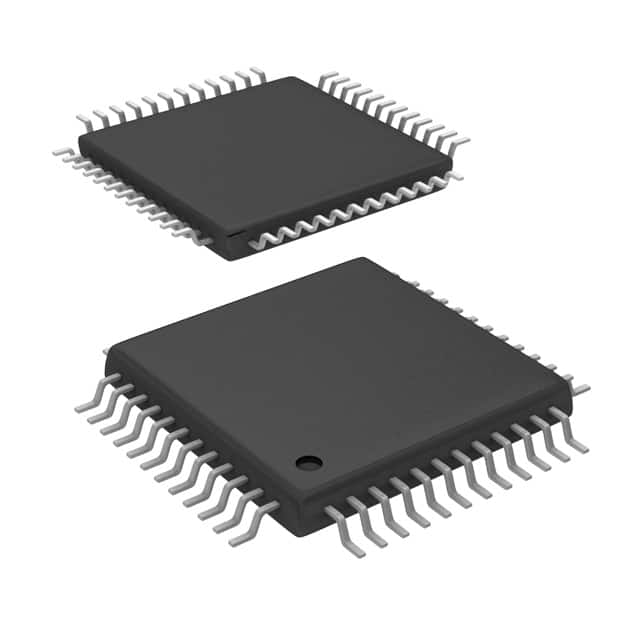
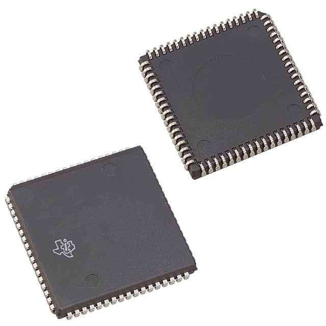
- Available in 48-Pin TQFP (PFB) Package, 32-Pin QFN (RHB), or 44-Pin PLCC (FN) Package
- Pin Compatible with TL16C752B (48-Pin Package PFB)


相關產品
| 製造商零件編號 | 價格(¥) | 現有數量 | |
|---|---|---|---|
 TL1431IZTIC VREF SHUNT ADJ 0.4% TO92-3 | 5.00 |
106
市場 | |
 TL1431IZIC VREF SHUNT ADJ 0.4% TO92-3 | 0.40 |
1165
市場 |
產品屬性
| 類型 | 描述 | 全選 |
|---|---|---|
| 帶自動流量控制 | 是 | |
| 電壓 - 供電 | 1.8V ~ 5V | |
| 數據速率(最大值) | 1.5Mbps | |
| FIFO | 16 字節 | |
| 供應商器件封裝 | 48-TQFP(7x7) | |
| 通道數 | 2,DUART | |
| 特性 | 內部振蕩器 | |
| 封裝/外殼 | 48-TQFP | |
| 產品狀態 | 在售 | |
| 安裝類型 | 表面貼裝型 | |
| 包裝 | 卷帶(TR) | |
| 帶調製解調器控制 | 是 | |
| 帶假起始位檢測 | 是 |
¥20.00
價格更新:一個月前
現貨供應:
1

Texas Instruments
德州儀器 (TI) 是一家開發模擬 IC 和嵌入式處理器的全球半導體設計和製造公司。 通過聘用世界上最聰明的人才,TI 創造了塑造技術未來的創新。 今天,TI 正在幫助超過 100,000 家客户改變未來。
查看所有産品從 Texas Instruments


部落格


 我們是可靠的合作夥伴无论您是想减少延长的交货时间,还是寻找分配的、过时的和其他报废的电子元件、半导体和其他难以找到的电子元件,SZC 都有供应链专业知识来解决您的材料 短缺。 将 SZC 及其已建立的 OEM 和 EMS 社区作为您的合作伙伴,您可以在电子元件短缺情况对市场价格产生不利影响之前快速、谨慎地采购受限产品。
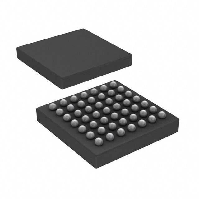 FPGA與微控制器:探索技術對決如果您想知道这两个电子巨头的差异、优点和缺点,那么您来对地方了。在本文中,我们将深入探讨 FPGA 与微控制器领域,揭示它们的优势所在,并揭示这一动态领域的领先厂商。
 晶片短缺對手機行業的影響智能手机行业正处于十字路口,在不断变化的市场动态中保持领先地位可以决定制造商的成功或失败。
 電晶體與電阻器:有什麼區別?在电子领域,晶体管和电阻器这两种重要元件发挥着独特但至关重要的作用。尽管尺寸不大,但这些元件却能够深刻地塑造电路和设备的行为。无论您是电子爱好者还是只是对技术感到好奇,了解晶体管和电阻器之间的差异都是一个很好的起点。
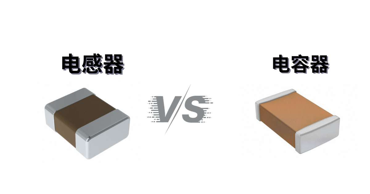 電感器與電容器:探索電力电感器和电容器可能不像华丽的处理器或耀眼的 LED 那样出名,但它们在让我们的小工具和小玩意运转方面发挥着至关重要的作用。在这个令人兴奋的旅程中,我们将深入了解电感器和电容器的世界,揭开它们的神秘面纱,探索它们的应用,并揭示它们之间的差异。我们还将为您提供有关维持电子世界运转的推荐制造商和分销商的内幕消息。
熱門製造商
View all manufactures 更多


熱門產品
更多電子零件 更多TL16C2550PFBR
IC DUAL UART 1.8V-5V FIFO 48TQFP
TL16C752BTPTREP
IC DUAL UART W/FIFO 3.3V 48-LQFP
NS16C2552TVA/NOPB
IC UART DUAL 16BYTE 44-PLCC

TL16C550CIPTR
IC ASYNC COMM ELEMENT 48-LQFP
TL16C554IPN
IC ASYNC COMM ELEMENT 80-LQFP

TL16C550DPTR
IC ASYNC COMM ELEMENT 48-LQFP

TL16C452FNR
IC ASYNC COMM ELEMENT 68-PLCC
TL16C752CIPFBRQ1
IC UART DUAL W/64B FIFO 48TQFP
TL16C754FN
IC QUAD UART 64BYTE FIFO 68PLCC

TL16C452FN
IC ASYNC COMM ELEMENT DUAL68PLCC