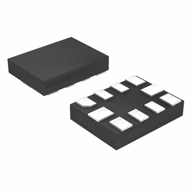
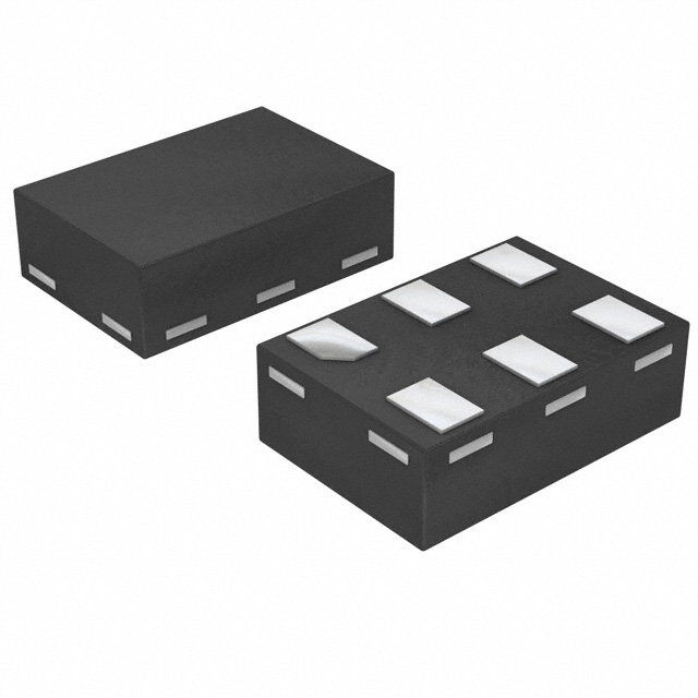
NX3L2267GM-Q100X
Compare
NX3L2267GM-Q100X
IC SWITCH SPDTX2 750MOHM 10XQFN


Compare


45
Serves customers in 45 countries
1000+
Worldwide Manufacturers
$140M
$140M Growth in 5 Years
50.0M+
50M Parts Shipped in 5 Years
The NX3L2267GM-Q100X is a dual low-ohmic single-pole double-throw analog switch suitable for use as an analog or digital 2:1 multiplexer/demultiplexer. Each switch has a digital select input (nS), two independent inputs/outputs (nY0 and nY1) and a common input/output (nZ).
Schmitt trigger action at the digital inputs makes the circuit tolerant to slower input rise and fall times. Low threshold digital inputs allows this device to be driven by 1.8 V logic levels in 3.3 V applications without significant increase in supply current ICC. This makes it possible for the NX3L2267GM-Q100X to switch 4.3 V signals with a 1.8 V digital controller, eliminating the need for logic level translation. The NX3L2267GM-Q100X allows signals with amplitude up to VCC to be transmitted from nZ to nY0 or nY1, or from nY0 or nY1 to nZ. Its low ON resistance (0.5 Ω) and flatness (0.13 Ω) ensures minimal attenuation and distortion of transmitted signals.
Feature
- Wide supply voltage range from 1.4 V to 4.3 V
- Very low ON resistance (peak):
- 1.65 Ω (typical) at VCC = 1.4 V
- 0.95 Ω (typical) at VCC = 1.65 V
- 0.55 Ω (typical) at VCC = 2.3 V
- 0.50 Ω (typical) at VCC = 2.7 V
- 0.50 Ω (typical) at VCC = 4.3 V
- Break-before-make switching
- High noise immunity
- ESD protection:
- HBM JESD22-A114F Class 3A exceeds 7500 V
- MM JESD22-A115-A exceeds 200 V
- CDM AEC-Q100-011 revision B exceeds 1000 V
- IEC61000-4-2 contact discharge exceeds 6000 V for switch ports
- CMOS low-power consumption
- Latch-up performance exceeds 100 mA per JESD 78B Class II Level A
- 1.8 V control logic at VCC = 3.6 V
- Control input accepts voltages above supply voltage
- Very low supply current, even when input is below VCC
- High current handling capability (350 mA continuous current under 3.3 V supply)
- Specified from -40 °C to +85 °C and from -40 °C to +125 °C
- Cell phone
- PDA
- Portable media player


Related Products
| Mfr Part # | Price ($) | Quantity Available | |
|---|---|---|---|
 NX3L1G384GW,125IC SW SPST-NCX1 750MOHM 5TSSOP | 0.14 |
3492
Marketplace | |
 NX3DV3899GU,115IC SWITCH DPDT X 2 3.3OHM 16XQFN | 0.69 |
6919
Marketplace |
Product Attributes
| TYPE | DESCRIPTION | Select all |
|---|---|---|
| Series | Automotive, AEC-Q100 | |
| Package | Tape & Reel (TR) | |
| Product Status | Obsolete | |
| Switch Circuit | SPDT | |
| Multiplexer/Demultiplexer Circuit | 2:1 | |
| Number of Circuits | 2 | |
| On-State Resistance (Max) | 750mOhm | |
| Channel-to-Channel Matching (ΔRon) | 90mOhm | |
| Voltage - Supply, Single (V+) | 1.4V ~ 4.3V | |
| Switch Time (Ton, Toff) (Max) | 40ns, 20ns | |
| -3db Bandwidth | 60MHz | |
| Charge Injection | 37pC | |
| Channel Capacitance (CS(off), CD(off)) | 35pF | |
| Current - Leakage (IS(off)) (Max) | 10nA | |
| Crosstalk | -90dB @ 100kHz | |
| Operating Temperature | -40°C ~ 125°C (TA) | |
| Mounting Type | Surface Mount | |
| Package / Case | 10-XFQFN | |
| Supplier Device Package | 10-XQFN (1.55x2) |
Price negotiable
Price update:a months ago
Available in stock:
3357

NXP USA Inc.
NXP Semiconductors, a frontrunner in embedded controllers, offers a wide array of MCUs with Arm-based processors. Their innovation extends to robust Power Management for industry and automotive use. NXP's products globally empower and interconnect, fostering proficiency for individuals, organizations, and the world. Noteworthy is the integration of Freescale Semiconductor into NXP (December 2015).
View All Product from NXP USA Inc.


Blog


 Unveiling the Future: The Surge of Microcontrollers in 2024In the dynamic world of electronic components, microcontrollers stand out as a testament to innovation and versatility. As we edge closer to 2024, the landscape for microcontrollers and semiconductors, spearheaded by giants like STMicroelectronics, Texas Instruments, and Microchip, is set for remarkable transformation.
 Microcontrollers vs. Microprocessors: Unveiling the Core Differences for Embedded Systems EngineeringSeasoned professionals in the realm of embedded systems engineering and product development within the electronics sphere often grapple with distinguishing between microcontrollers and microprocessors. Despite their foundational role in the design and fabrication of a myriad of electronic gadgets, understanding their unique functionalities based on mere definitions can be challenging:
 A Deep Dive into the Global Ceramic Capacitors MarketJoin us in exploring the emerging subplot of environmental consciousness within the global ceramic capacitors market.
 Mastering Current Measurement with MicrocontrollersUnlock precise current measurement secrets with Microcontrollers! Conquer challenges, meet superhero solutions, and revolutionize accuracy with on-chip Analog Core Independent Peripherals (CIPs).
 What is a Rectifier Diode: A Guide to BeginnersMeet the unsung heroes of electronics—Rectifier Diodes! Explore their magic, applications, and join the behind-the-scenes adventure into gadget power.


Popular Manufacturers
View all manufactures More


Popular Parts Number
More Electronic Parts More
NX3L4684TK,115
IC SWITCH SPDTX2 750MOHM 10HVSON
NX3L4053HR-Q100115
MULTIPLEXERS/SWITCHES, 3 FUNC, C
NX3L2T66GM,125
IC SW SPST-NOX2 750MOHM 8XQFNU
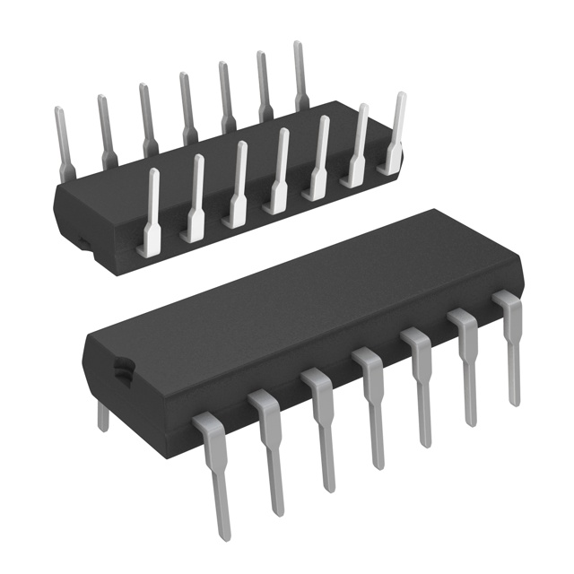
HEF4016BP,652
IC SWITCH SPST-NOX4 350OHM 14DIP

74HC4316N,652
IC SWITCH SPST-NOX4 135OHM 16DIP

74HC4066N,652
IC SWITCH SPST-NOX4 95OHM 14DIP
NX3V1T66GM,132
IC SW SPST-NOX1 450MOHM 6XSON

NX3V1G66GM,132
IC SW SPST-NOX1 450MOHM 6XSON
NX3L1G384GW,125
IC SW SPST-NCX1 750MOHM 5TSSOP
NX3L1G53GD,125
IC SWITCH SPDT X 1 750MOHM 8XSON