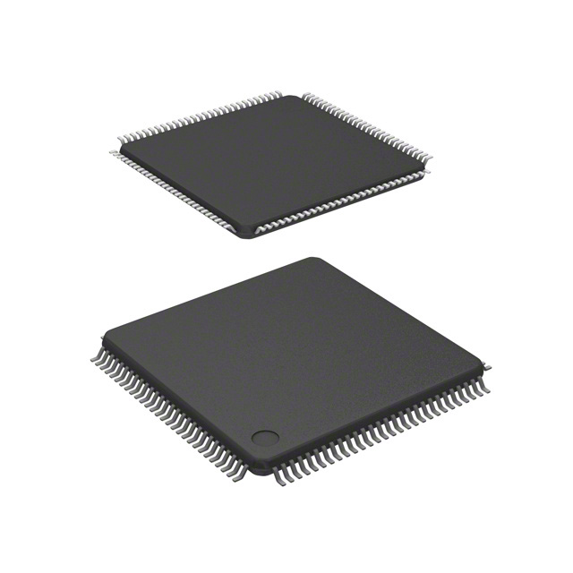
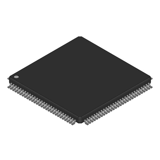
MC9S12DT128CPVE
Compare
MC9S12DT128CPVE
IC MCU 16BIT 128KB FLASH 112LQFP


Compare


45
Serves customers in 45 countries
1000+
Worldwide Manufacturers
$140M
$140M Growth in 5 Years
50.0M+
50M Parts Shipped in 5 Years
Designed for automotive multiplexing applications, members of the MC9S12DT128CPVE of 16 bit Flash based microcontrollers are fully pin compatible and enable users to choose between different memory and peripheral options for scalable designs. All MC9S12DT128CPVE devices are composed of standard on-chip peripherals including a 16-bit central processing unit (CPU12), up to 512K bytes of Flash EEPROM, 14K bytes of RAM, 4K bytes of EEPROM, two asynchronous serial communications interfaces (SCI), three serial peripheral interfaces (SPI), IIC-bus, an enhanced capture timer (ECT), two 8-channel 10-bit analog-to-digital converters (ADC), an eight-channel pulse-width modulator (PWM), J1850 interface and up to five CAN 2.0 A, B software compatible modules (MSCAN12). System resource mapping, clock generation, interrupt control and bus interfacing are managed by the system integration module (SIM).
The MC9S12DT128CPVE has full 16-bit data paths throughout, however, the external bus can operate in an 8-bit narrow mode so single 8-bit wide memory can be interfaced for lower cost systems. The inclusion of a PLL circuit allows power consumption and performance to be adjusted to suit operational requirements. In addition to the I/O ports available in each module, up to 22 I/O ports are available with interrupt capability allowing Wake-Up from STOP or WAIT mode.
Feature
• 16-bit CPU12
— Upward compatible with M68HC11 instruction set
— Interrupt stacking and programmer’s model identical to M68HC11
— HCS12 Instruction queue
— Enhanced indexed addressing
• Multiplexed bus
— Single chip or expanded
— 16 address/16 data wide or 16 address/8 data narrow modes
— External address space 1MByte for Data and Program space (112 pin package only)
• Wake-up interrupt inputs depending on the package option
— 8-bit port H
— 2-bit port J1:0
— 2-bit port J7:6 shared with IIC, CAN4 and CAN0 module
— 8-bit port P shared with PWM or SPI1,2
• Memory options
— 32K, 64K, 128K, 256K, 512K Byte Flash EEPROM
— 1K, 2K, 4K Byte EEPROM
— 2K, 4K, 8K, 12K, 14K Byte RAM
• Analog-to-Digital Converters
— One or two 8-channel modules with 10-bit resolution depending on the package option
— External conversion trigger capability
• Up to five 1M bit per second, CAN 2.0 A, B software compatible modules
— Five receive and three transmit buffers
— Flexible identifier filter programmable as 2 x 32 bit, 4 x 16 bit or 8 x 8 bit
— Four separate interrupt channels for Receive, Transmit, Error and Wake-up
— Low-pass filter wake-up function in STOP mode
— Loop-back for self test operation
• Enhanced Capture Timer (ECT)
— 16-bit main counter with 7-bit prescaler
— 8 programmable input capture or output compare channels; 4 of the 8 input captures with buffer
— Input capture filters and buffers, three successive captures on four channels, or two captures on four channels with a capture/compare selectable on the remaining four
— Four 8-bit or two 16-bit pulse accumulators
— 16-bit modulus down-counter with 4-bit prescaler
— Four user-selectable delay counters for signal filtering
• 8 PWM channels with programmable period and duty cycle (7 channels on 80 Pin Packages)
— 8-bit, 8-channel or 16-bit, 4-channel
— Separate control for each pulse width and duty cycle
— Center- or left-aligned outputs
— Programmable clock select logic with a wide range of frequencies
• Serial interfaces
— Two asynchronous serial communications interfaces (SCI)
— Up to three synchronous serial peripheral interfaces (SPI)
— IIC
• SAE J1850 Compatible Module (BDLC)
— 10.4 kbps Variable Pulse Width format
— Byte level receive and transmit
— 4x receive mode supported
• SIM (System Integration Module)
— CRG (windowed COP watchdog, real time interrupt, clock monitor, clock generation and reset)
— MEBI (multiplexed external bus interface)
— INT (interrupt control)
• Clock generation
— Phase-locked loop clock frequency multiplier
— Limp home mode in absence of external clock
— Clock Monitor
— Low power 0.5 to 16 MHz crystal oscillator reference clock
• Operating frequency for ambient temperatures TA -40°C <= TA <= 125°C
— 50MHz equivalent to 25MHz Bus Speed for single chip 40MHz equivalent to 20MHz Bus Speed in expanded bus modes.
• Internal 5V to 2.5V Regulator
• 112-Pin LQFP or 80-Pin QFP package
— I/O lines with 5V input and drive capability
— 5V A/D converter inputs and 5V I/O
— 2.5V logic supply
• Development support
— Single-wire background debug™ mode (BDM)
— On-chip hardware breakpoints


Related Products
| Mfr Part # | Price ($) | Quantity Available | |
|---|---|---|---|
 MC9S12DT128CPVIC MCU 16BIT 128KB FLASH 112LQFP | Price negotiable |
3964
Marketplace |
Product Attributes
| TYPE | DESCRIPTION | Select all |
|---|---|---|
| Series | HCS12 | |
| Package | Tray | |
| Product Status | Active | |
| Programmable | Verified | |
| Core Processor | HCS12 | |
| Core Size | 16-Bit | |
| Speed | 25MHz | |
| Connectivity | CANbus, I²C, SCI, SPI | |
| Peripherals | PWM, WDT | |
| Number of I/O | 91 | |
| Program Memory Size | 128KB (128K x 8) | |
| Program Memory Type | FLASH | |
| EEPROM Size | 2K x 8 | |
| RAM Size | 8K x 8 | |
| Voltage - Supply (Vcc/Vdd) | 2.35V ~ 5.25V | |
| Data Converters | A/D 16x10b | |
| Oscillator Type | Internal | |
| Operating Temperature | -40°C ~ 85°C (TA) | |
| Mounting Type | Surface Mount | |
| Package / Case | 112-LQFP | |
| Supplier Device Package | 112-LQFP (20x20) |
$68.95
Price update:a months ago
Available in stock:
4263

NXP USA Inc.
NXP Semiconductors, a frontrunner in embedded controllers, offers a wide array of MCUs with Arm-based processors. Their innovation extends to robust Power Management for industry and automotive use. NXP's products globally empower and interconnect, fostering proficiency for individuals, organizations, and the world. Noteworthy is the integration of Freescale Semiconductor into NXP (December 2015).
View All Product from NXP USA Inc.


Blog


 Unveiling the Future: The Surge of Microcontrollers in 2024In the dynamic world of electronic components, microcontrollers stand out as a testament to innovation and versatility. As we edge closer to 2024, the landscape for microcontrollers and semiconductors, spearheaded by giants like STMicroelectronics, Texas Instruments, and Microchip, is set for remarkable transformation.
 Microcontrollers vs. Microprocessors: Unveiling the Core Differences for Embedded Systems EngineeringSeasoned professionals in the realm of embedded systems engineering and product development within the electronics sphere often grapple with distinguishing between microcontrollers and microprocessors. Despite their foundational role in the design and fabrication of a myriad of electronic gadgets, understanding their unique functionalities based on mere definitions can be challenging:
 A Deep Dive into the Global Ceramic Capacitors MarketJoin us in exploring the emerging subplot of environmental consciousness within the global ceramic capacitors market.
 Mastering Current Measurement with MicrocontrollersUnlock precise current measurement secrets with Microcontrollers! Conquer challenges, meet superhero solutions, and revolutionize accuracy with on-chip Analog Core Independent Peripherals (CIPs).
 What is a Rectifier Diode: A Guide to BeginnersMeet the unsung heroes of electronics—Rectifier Diodes! Explore their magic, applications, and join the behind-the-scenes adventure into gadget power.


Popular Manufacturers
View all manufactures More


Popular Parts Number
More Electronic Parts MoreMC9S12DT128CPVE
IC MCU 16BIT 128KB FLASH 112LQFP
S908QY4E0CDWER
MICROCONTROLLER, 8 BIT, HC08/S08

MC9S08RC8FJE
IC MCU 8BIT 8KB FLASH 32LQFP
MC9S12XD64MAA
IC MCU 16BIT 64KB FLASH 80QFP

MC9S12B128VPV
MICROCONTROLLER
MC9S12HZ128CAL
IC MCU 16BIT 128KB FLASH 112LQFP
SPC5553MVR132
IC MCU 32BIT 1.5KB FLASH 416PBGA
MC9RS08LA8CLF
IC MCU 8BIT 8KB FLASH 48LQFP
MCF52211CVM66
RISC MICROCONTROLLER, 32-BIT, FL
MC9S08JM8CGT
IC MCU 8BIT 8KB FLASH 48QFN