


面议
价格更新:一个月前
现货供应:
3075


45
为45个国家的客户提供服务
1000+
全球制造商
$140M
5年增长1.4亿美元
50.0M+
5年内配送了5000万个元件

Lattice Semiconductor Corporation
Lattice Semiconductor 是低功耗可编程的领导者。 在不断增长的通信、计算、工业、汽车和消费市场中,他们通过网络解决客户问题,从边缘到云端。 他们的技术、长期合作关系以及对世界级支持的承诺让他们的客户能够快速、轻松地释放他们的创新,以创造一个智能、安全和互联的世界。
查看所有产品从 Lattice Semiconductor Corporation


The LatticeECP/EC family of FPGA devices has been optimized to deliver mainstream FPGA features at low cost. For maximum performance and value, the LatticeECP (EConomy Plus) FPGA concept combines an efficient FPGA fabric with high-speed dedicated functions. Lattice’s first family to implement this approach is the LatticeECP-DSP (EConomy Plus DSP) family, providing dedicated high-performance DSP blocks on-chip. The LatticeEC™ (EConomy) family supports all the general purpose features of LatticeECP devices without dedicated function blocks to achieve lower cost solutions.
The LatticeECP/EC FPGA fabric, which was designed from the outset with low cost in mind, contains all the critical FPGA elements: LUT-based logic, distributed and embedded memory, PLLs and support for mainstream I/Os. Dedicated DDR memory interface logic is also included to support this memory that is becoming increasingly prevalent in cost-sensitive applications.
The ispLEVER® design tool from Lattice allows large complex designs to be efficiently implemented using the LatticeECP/EC family of FPGA devices. Synthesis library support for LatticeECP/EC is available for popular logic synthesis tools. The ispLEVER tool uses the synthesis tool output along with the constraints from its floor planning tools to place and route the design in the LatticeECP/EC device. The ispLEVER tool extracts the timing from the routing and back-annotates it into the design for timing verification.
Lattice provides many pre-designed IP (Intellectual Property) ispLeverCORE™ modules for the LatticeECP/EC family. By using these IPs as standardized blocks, designers are free to concentrate on the unique aspects of their design, increasing their productivity.
Feature
■ Extensive Density and Package Options
• 1.5K to 41K LUT4s
• 65 to 576 I/Os
• Density migration supported
■ sysDSP™ Block (LatticeECP™ Versions)
• High performance multiply and accumulate
• 4 to 10 blocks
− 4 to 10 36x36 multipliers or
– 16 to 40 18x18 multipliers or
− 32 to 80 9x9 multipliers
■ Embedded and Distributed Memory
• 18 Kbits to 645 Kbits sysMEM™ Embedded Block RAM (EBR)
• Up to 163 Kbits distributed RAM
• Flexible memory resources:
− Distributed and block memory
■ Flexible I/O Buffer
• Programmable sysIO™ buffer supports wide range of interfaces:
− LVCMOS 3.3/2.5/1.8/1.5/1.2
− LVTTL − SSTL 3/2 Class I, II, SSTL18 Class I
− HSTL 18 Class I, II, III, HSTL15 Class I, III
− PCI
− LVDS, Bus-LVDS, LVPECL, RSDS
■ Dedicated DDR Memory Support
• Implements interface up to DDR400 (200MHz)
■ sysCLOCK™ PLLs
• Up to 4 analog PLLs per device
• Clock multiply, divide and phase shifting
■ System Level Support
• IEEE Standard 1149.1 Boundary Scan, plus ispTRACY™ internal logic analyzer capability
• SPI boot flash interface
• 1.2V power supply
■ Low Cost FPGA
• Features optimized for mainstream applications
• Low cost TQFP and PQFP packaging


相关产品
| 制造商零件编号 | 价格(¥) | 现有数量 | |
|---|---|---|---|
 LFEC10E-3FN484IIC FPGA 288 I/O 484FBGA | 85.00 |
2250
市场 | |
 LFEC3E-3TN144CIC FPGA 97 I/O 144TQFP | 25.00 |
4920
市场 | |
 LFEC3E-5Q208CIC FPGA 145 I/O 208QFP | 面议 |
2383
市场 | |
 LFEC3E-4TN144CIC FPGA 97 I/O 144TQFP | 10.00 |
2278
市场 |
产品属性
| 类型 | 描述 | 全选 |
|---|---|---|
| 电压 - 供电 | 1.14V ~ 1.26V | |
| 安装类型 | 表面贴装型 | |
| 系列 | ECP | |
| 工作温度 | 0°C ~ 85°C(TJ) | |
| 包装 | 托盘 | |
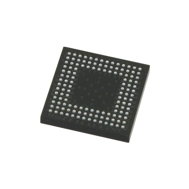
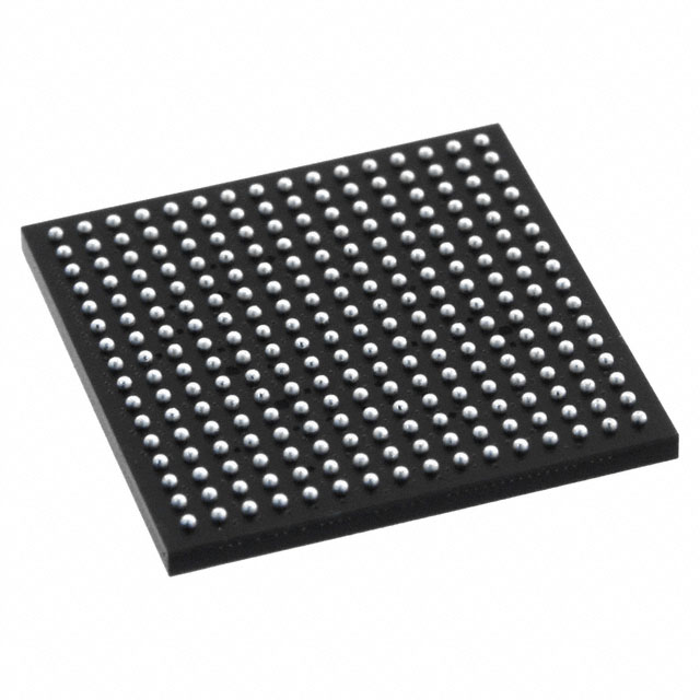
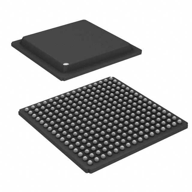
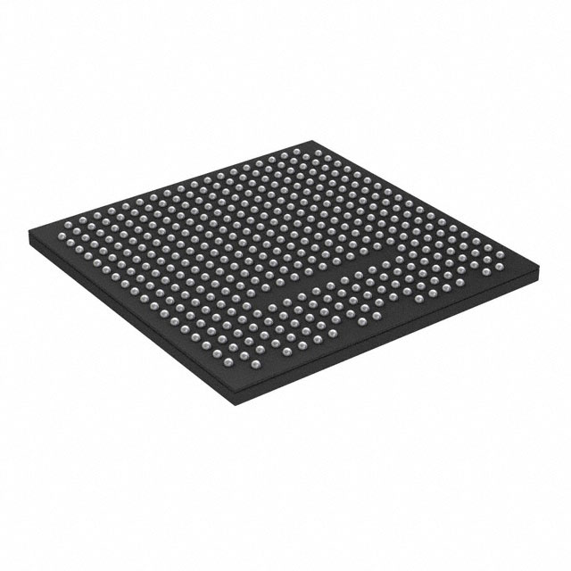
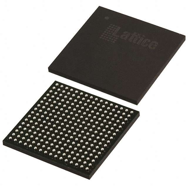
| 封装/外壳 | 256-BGA | |
| 产品状态 | 停产 | |
| 供应商器件封装 | 256-FPBGA(17x17) | |
| 可编程 | 未验证 | |
| 逻辑元件/单元数 | 10200 | |
| 总 RAM 位数 | 282624 | |
| I/O 数 | 195 |
博客
 深入探讨全球陶瓷电容器市场加入我们,一起探索全球陶瓷电容器市场中的最新趋势。
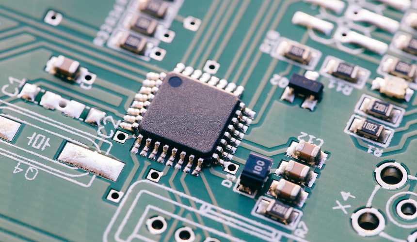 掌握使用微控制器进行电流测量与与模数转换器 (ADC) 顺利配合的电压不同,电流测量增加了一层复杂性,可能导致不准确。对当前测量细微差别的探索将揭示这些误差的根源,并引入超级英雄解决方案:片上模拟核心独立外设 (CIP)。
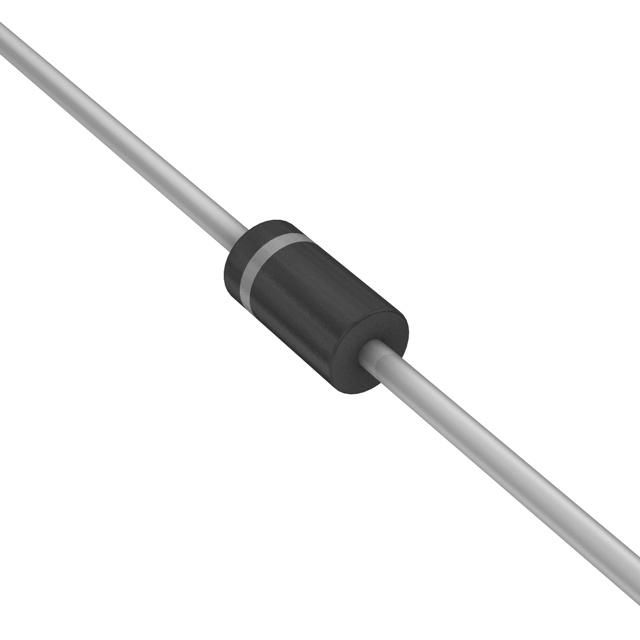 什么是整流二极管:初学者指南揭开整流二极管的秘密!链接整流二极管的定义,应用领域,工作原理,以及常见的整流二极管。
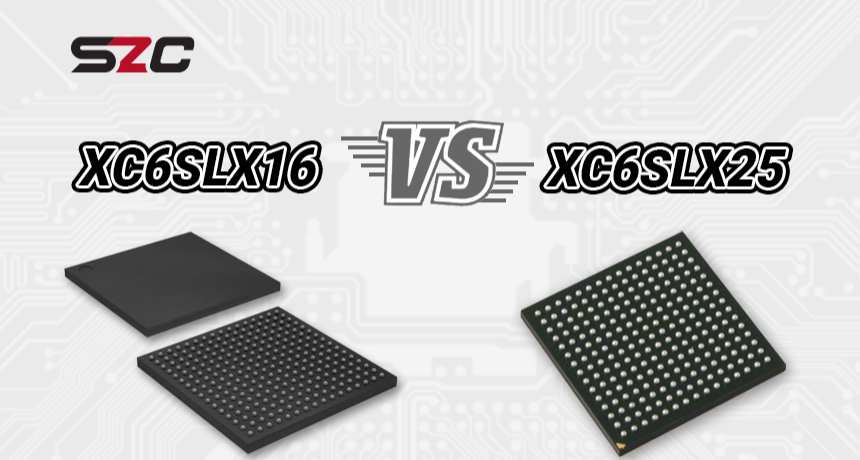 FPGA对比:XC6SLX16 vs. XC6SLX25通过我们的快速指南解锁fpga的秘密!XC6SLX16或xc6slx25 -哪一款是您下一次科技冒险的关键?点击现在探索可编程可能性的世界!
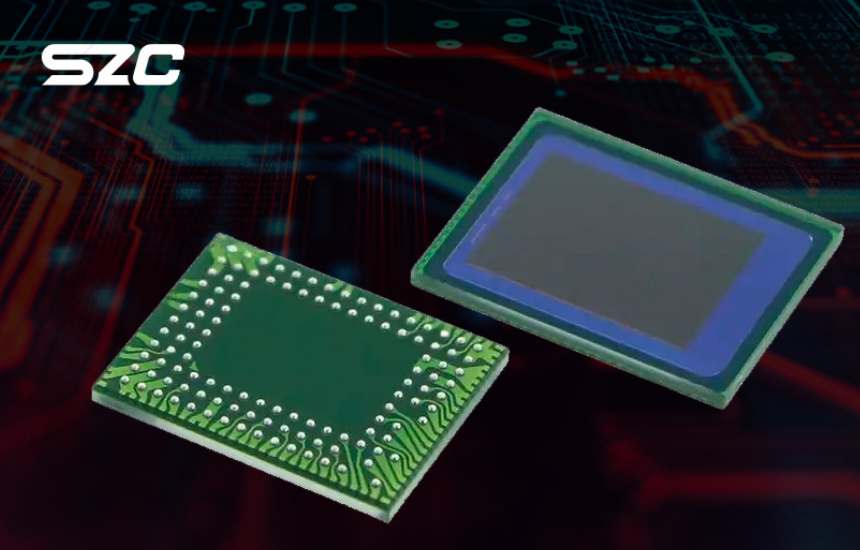 利用onsemi的先进图像传感器增强道路安全来看看onsemi的AR0220AT吧,它是高级驾驶辅助系统(Advanced Driver Assistance Systems)中的一款夜间智能游戏颠覆者。
面议
价格更新:一个月前
现货供应:
3075
Lattice Semiconductor Corporation
Lattice Semiconductor 是低功耗可编程的领导者。 在不断增长的通信、计算、工业、汽车和消费市场中,他们通过网络解决客户问题,从边缘到云端。 他们的技术、长期合作关系以及对世界级支持的承诺让他们的客户能够快速、轻松地释放他们的创新,以创造一个智能、安全和互联的世界。
查看所有产品从 Lattice Semiconductor Corporation博客
- 深入探讨全球陶瓷电容器市场加入我们,一起探索全球陶瓷电容器市场中的最新趋势。
- 掌握使用微控制器进行电流测量与与模数转换器 (ADC) 顺利配合的电压不同,电流测量增加了一层复杂性,可能导致不准确。对当前测量细微差别的探索将揭示这些误差的根源,并引入超级英雄解决方案:片上模拟核心独立外设 (CIP)。
- 什么是整流二极管:初学者指南揭开整流二极管的秘密!链接整流二极管的定义,应用领域,工作原理,以及常见的整流二极管。
- FPGA对比:XC6SLX16 vs. XC6SLX25通过我们的快速指南解锁fpga的秘密!XC6SLX16或xc6slx25 -哪一款是您下一次科技冒险的关键?点击现在探索可编程可能性的世界!
- 利用onsemi的先进图像传感器增强道路安全来看看onsemi的AR0220AT吧,它是高级驾驶辅助系统(Advanced Driver Assistance Systems)中的一款夜间智能游戏颠覆者。
热门制造商
View all manufactures 更多


热门产品
更多电子零件 更多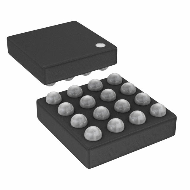
ICE40LP640-SWG16TR1K
IC FPGA 10 I/O 16WLCSP
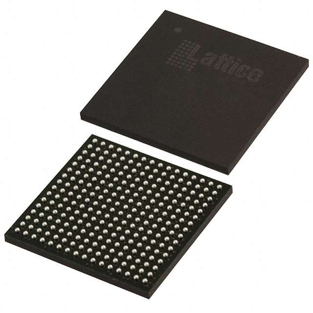
LCMXO2-7000ZE-1FTG256I
IC FPGA 206 I/O 256FTBGA
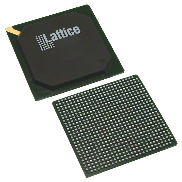
LFE3-70EA-6LFN672I
IC FPGA 380 I/O 672FPBGA
OR2C26A3PS208-N-DB
FIELD PROGRAMMABLE GATE ARRAY
LCMXO2-1200ZE-3MG132I
IC FPGA 104 I/O 132CSBGA
LFXP2-17E-7FTN256C
IC FPGA 201 I/O 256FTBGA
LCMXO2280C-3FTN256I
IC FPGA 211 I/O 256FTBGA

LCMXO2-256ZE-1MG132C
IC FPGA 55 I/O 132CSBGA
LAE5UM-45F-7BG381E
IC FPGA 203 I/O 381CABGA
LCMXO2-2000HE-4FTG256I
IC FPGA 206 I/O 256FTBGA