
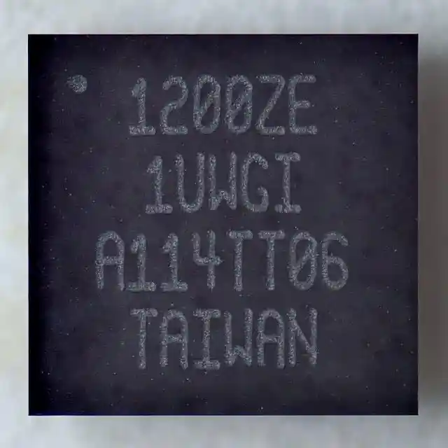
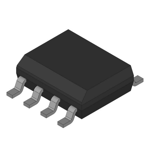
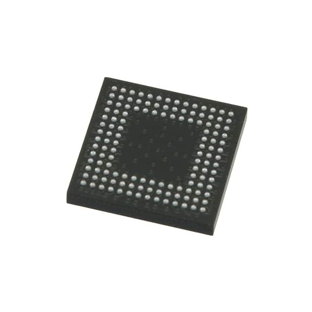
LCMXO2-1200ZE-1UWG25ITR
对比
LCMXO2-1200ZE-1UWG25ITR
IC FPGA 18 I/O 25WLCSP


对比
¥150.00
价格更新:一个月前
现货供应:
20000


45
为45个国家的客户提供服务
1000+
全球制造商
$140M
5年增长1.4亿美元
50.0M+
5年内配送了5000万个元件

Lattice Semiconductor Corporation
Lattice Semiconductor 是低功耗可编程的领导者。 在不断增长的通信、计算、工业、汽车和消费市场中,他们通过网络解决客户问题,从边缘到云端。 他们的技术、长期合作关系以及对世界级支持的承诺让他们的客户能够快速、轻松地释放他们的创新,以创造一个智能、安全和互联的世界。
查看所有产品从 Lattice Semiconductor Corporation


Feature
Flexible Logic Architecture
• Six devices with 256 to 6864 LUT4s and 19 to 335 I/Os
Ultra Low Power Devices
• Advanced 65 nm low power process
• As low as 19 µW standby power
• Programmable low swing differential I/Os
• Stand-by mode and other power saving options
Embedded and Distributed Memory
• Up to 240 Kbits sysMEM™ Embedded Block RAM
• Up to 54 Kbits Distributed RAM
• Dedicated FIFO control logic
On-Chip User Flash Memory
• Up to 256 Kbits of User Flash Memory
• 100,000 write cycles
• Accessible through WISHBONE, SPI, I2 C and JTAG interfaces
• Can be used as soft processor PROM or as Flash memory
Pre-Engineered Source Synchronous I/O
• DDR registers in I/O cells
• Dedicated gearing logic
• 7:1 Gearing for Display I/Os
• Generic DDR, DDRX2, DDRX4
• Dedicated DDR/DDR2/LPDDR memory with DQS support
High Performance, Flexible I/O Buffer
• Programmable sysIO™ buffer supports wide range of interfaces:
– LVCMOS 3.3/2.5/1.8/1.5/1.2
– LVTTL
– PCI
– LVDS, Bus-LVDS, MLVDS, RSDS, LVPECL
– SSTL 25/18
– HSTL 18
– Schmitt trigger inputs, up to 0.5V hysteresis
• I/Os support hot socketing
• On-chip differential termination
• Programmable pull-up or pull-down mode
Flexible On-Chip Clocking
• Eight primary clocks
• Up to two edge clocks for high-speed I/O interfaces (top and bottom sides only)
• Up to two analog PLLs per device with fractional-n frequency synthesis – Wide input frequency range (10 MHz to 400 MHz)
Non-volatile, Infinitely Reconfigurable
• Instant-on – powers up in microseconds
• Single-chip, secure solution
• Programmable through JTAG, SPI or I2 C
• Supports background programming of non-volatile memory
• Optional dual boot with external SPI memory
TransFR™ Reconfiguration
• In-field logic update while system operates
Enhanced System Level Support
• On-chip hardened functions: SPI, I2 C, timer/ counter
• On-chip oscillator with 5.5% accuracy
• Unique TraceID for system tracking
• One Time Programmable (OTP) mode
• Single power supply with extended operating range
• IEEE Standard 1149.1 boundary scan
• IEEE 1532 compliant in-system programming
Broad Range of Package Options
• TQFP, WLCSP, ucBGA, csBGA, caBGA, ftBGA, fpBGA, QFN package options
• Small footprint package options – As small as 2.5x2.5mm
• Density migration supported
• Advanced halogen-free packaging


产品属性
| 类型 | 描述 | 全选 |
|---|---|---|
| 系列 | MachXO2 | |
| 包装 | 卷带(TR) | |
| 产品状态 | 在售 | |
| 可编程 | 未验证 | |
| LAB/CLB 数 | 160 | |
| 逻辑元件/单元数 | 1280 | |
| 总 RAM 位数 | 65536 | |
| I/O 数 | 18 | |
| 电压 - 供电 | 1.14V ~ 1.26V | |
| 安装类型 | 表面贴装型 | |
| 工作温度 | -40°C ~ 100°C(TJ) | |
| 封装/外壳 | 25-UFBGA,WLCSP | |
| 供应商器件封装 | 25-WLCSP |
博客
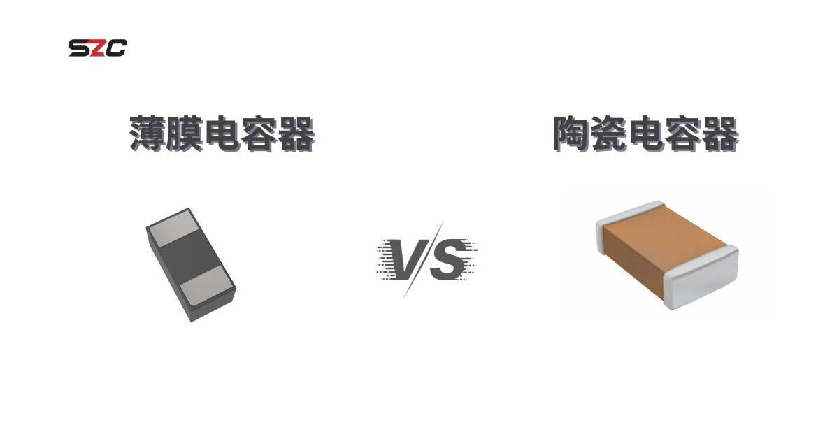
 深入探讨全球陶瓷电容器市场加入我们,一起探索全球陶瓷电容器市场中的最新趋势。
 掌握使用微控制器进行电流测量与与模数转换器 (ADC) 顺利配合的电压不同,电流测量增加了一层复杂性,可能导致不准确。对当前测量细微差别的探索将揭示这些误差的根源,并引入超级英雄解决方案:片上模拟核心独立外设 (CIP)。
 什么是整流二极管:初学者指南揭开整流二极管的秘密!链接整流二极管的定义,应用领域,工作原理,以及常见的整流二极管。
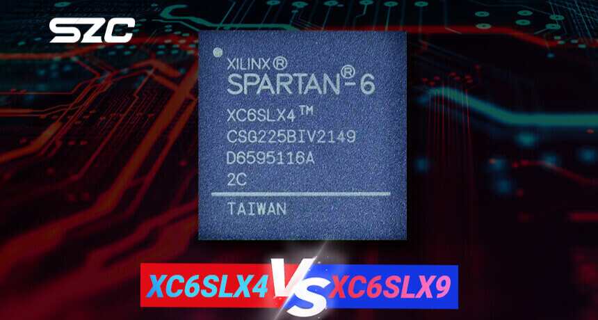
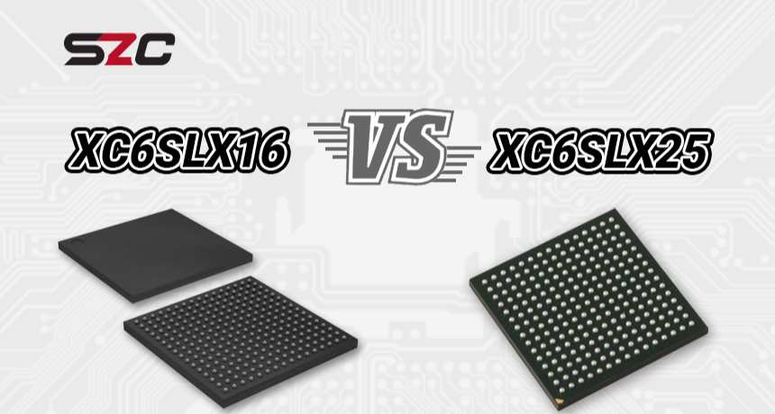 FPGA对比:XC6SLX16 vs. XC6SLX25通过我们的快速指南解锁fpga的秘密!XC6SLX16或xc6slx25 -哪一款是您下一次科技冒险的关键?点击现在探索可编程可能性的世界!
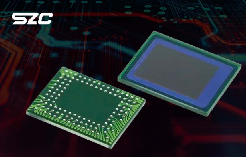 利用onsemi的先进图像传感器增强道路安全来看看onsemi的AR0220AT吧,它是高级驾驶辅助系统(Advanced Driver Assistance Systems)中的一款夜间智能游戏颠覆者。
¥150.00
价格更新:一个月前
现货供应:
20000
Lattice Semiconductor Corporation
Lattice Semiconductor 是低功耗可编程的领导者。 在不断增长的通信、计算、工业、汽车和消费市场中,他们通过网络解决客户问题,从边缘到云端。 他们的技术、长期合作关系以及对世界级支持的承诺让他们的客户能够快速、轻松地释放他们的创新,以创造一个智能、安全和互联的世界。
查看所有产品从 Lattice Semiconductor Corporation博客
- 深入探讨全球陶瓷电容器市场加入我们,一起探索全球陶瓷电容器市场中的最新趋势。
- 掌握使用微控制器进行电流测量与与模数转换器 (ADC) 顺利配合的电压不同,电流测量增加了一层复杂性,可能导致不准确。对当前测量细微差别的探索将揭示这些误差的根源,并引入超级英雄解决方案:片上模拟核心独立外设 (CIP)。
- 什么是整流二极管:初学者指南揭开整流二极管的秘密!链接整流二极管的定义,应用领域,工作原理,以及常见的整流二极管。
- FPGA对比:XC6SLX16 vs. XC6SLX25通过我们的快速指南解锁fpga的秘密!XC6SLX16或xc6slx25 -哪一款是您下一次科技冒险的关键?点击现在探索可编程可能性的世界!
- 利用onsemi的先进图像传感器增强道路安全来看看onsemi的AR0220AT吧,它是高级驾驶辅助系统(Advanced Driver Assistance Systems)中的一款夜间智能游戏颠覆者。
热门制造商
View all manufactures 更多


热门产品
更多电子零件 更多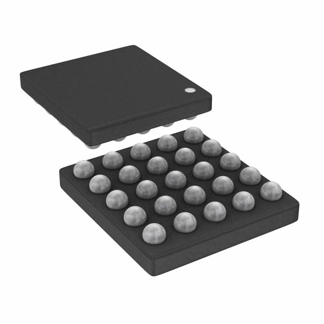
LCMXO2-1200ZE-1UWG25ITR1K
IC FPGA 18 I/O 25WLCSP
LCMXO2-1200ZE-1UWG25ITR
IC FPGA 18 I/O 25WLCSP
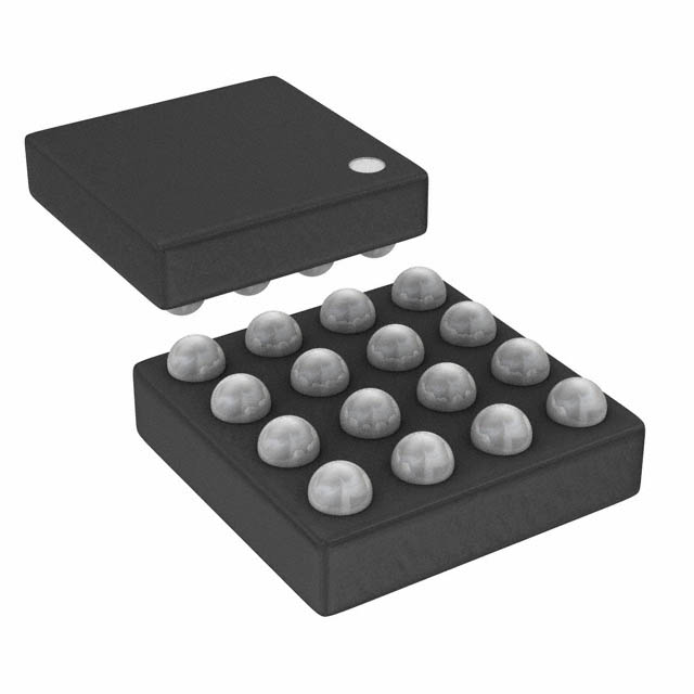
ICE40LP640-SWG16TR1K
IC FPGA 10 I/O 16WLCSP
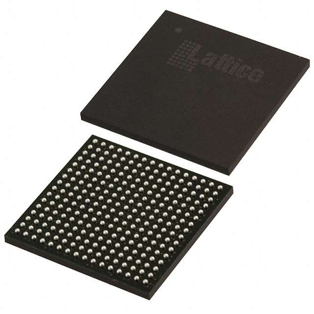
LCMXO2-7000ZE-1FTG256I
IC FPGA 206 I/O 256FTBGA
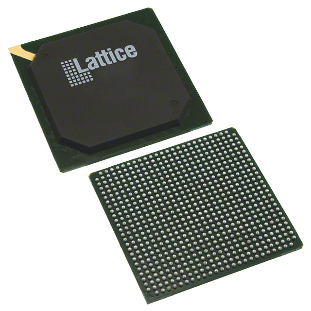
LFE3-70EA-6LFN672I
IC FPGA 380 I/O 672FPBGA
OR2C26A3PS208-N-DB
FIELD PROGRAMMABLE GATE ARRAY
LCMXO2-1200ZE-3MG132I
IC FPGA 104 I/O 132CSBGA
LFXP2-17E-7FTN256C
IC FPGA 201 I/O 256FTBGA
LCMXO2280C-3FTN256I
IC FPGA 211 I/O 256FTBGA

LCMXO2-256ZE-1MG132C
IC FPGA 55 I/O 132CSBGA