


面议
价格更新:一个月前
现货供应:
3574


45
为45个国家的客户提供服务
1000+
全球制造商
$140M
5年增长1.4亿美元
50.0M+
5年内配送了5000万个元件

Lattice Semiconductor Corporation
Lattice Semiconductor 是低功耗可编程的领导者。 在不断增长的通信、计算、工业、汽车和消费市场中,他们通过网络解决客户问题,从边缘到云端。 他们的技术、长期合作关系以及对世界级支持的承诺让他们的客户能够快速、轻松地释放他们的创新,以创造一个智能、安全和互联的世界。
查看所有产品从 Lattice Semiconductor Corporation


The LatticeECP3™ (EConomy Plus Third generation) family of FPGA devices is optimized to deliver high performance features such as an enhanced DSP architecture, high speed SERDES and high speed source synchronous interfaces in an economical FPGA fabric. This combination is achieved through advances in device architecture and the use of 65 nm technology making the devices suitable for high-volume, high-speed, low-cost applications.
The LatticeECP3 device family expands look-up-table (LUT) capacity to 149K logic elements and supports up to 586 user I/Os. The LatticeECP3 device family also offers up to 320 18 x 18 multipliers and a wide range of parallel I/O standards.
The LatticeECP3 FPGA fabric is optimized with high performance and low cost in mind. The LatticeECP3 devices utilize reconfigurable SRAM logic technology and provide popular building blocks such as LUT-based logic, distributed and embedded memory, Phase Locked Loops (PLLs), Delay Locked Loops (DLLs), pre-engineered source synchronous I/O support, enhanced sysDSP slices and advanced configuration support, including encryption and dual-boot capabilities.
The pre-engineered source synchronous logic implemented in the LatticeECP3 device family supports a broad range of interface standards, including DDR3, XGMII and 7:1 LVDS.
The LatticeECP3 device family also features high speed SERDES with dedicated PCS functions. High jitter tolerance and low transmit jitter allow the SERDES plus PCS blocks to be configured to support an array of popular data protocols including PCI Express, SMPTE, Ethernet (XAUI, GbE, and SGMII) and CPRI. Transmit Pre-emphasis and Receive Equalization settings make the SERDES suitable for transmission and reception over various forms of media.
The LatticeECP3 devices also provide flexible, reliable and secure configuration options, such as dual-boot capability, bit-stream encryption, and TransFR field upgrade features.
The Lattice Diamond™ and ispLEVER® design software allows large complex designs to be efficiently implemented using the LatticeECP3 FPGA family. Synthesis library support for LatticeECP3 is available for popular logic synthesis tools. Diamond and ispLEVER tools use the synthesis tool output along with the constraints from its floor planning tools to place and route the design in the LatticeECP3 device. The tools extract the timing from the routing and back-annotate it into the design for timing verification.
Lattice provides many pre-engineered IP (Intellectual Property) modules for the LatticeECP3 family. By using these configurable soft core IPs as standardized blocks, designers are free to concentrate on the unique aspects of their design, increasing their productivity.
Feature
Higher Logic Density for Increased System Integration
• 17K to 149K LUTs
• 116 to 586 I/Os Embedded SERDES
• 150 Mbps to 3.2 Gbps for Generic 8b10b, 10-bit SERDES, and 8-bit SERDES modes
• Data Rates 230 Mbps to 3.2 Gbps per channel for all other protocols
• Up to 16 channels per device: PCI Express, SONET/SDH, Ethernet (1GbE, SGMII, XAUI), CPRI, SMPTE 3G and Serial RapidIO
sysDSP™
• Fully cascadable slice architecture
• 12 to 160 slices for high performance multiply and accumulate
• Powerful 54-bit ALU operations
• Time Division Multiplexing MAC Sharing
• Rounding and truncation
• Each slice supports
— Half 36x36, two 18x18 or four 9x9 multipliers
— Advanced 18x36 MAC and 18x18 MultiplyMultiply-Accumulate (MMAC) operations
Flexible Memory Resources
• Up to 6.85Mbits sysMEM™ Embedded Block RAM (EBR)
• 36K to 303K bits distributed RAM
sysCLOCK Analog PLLs and DLLs
• Two DLLs and up to ten PLLs per device
Pre-Engineered Source Synchronous I/O
• DDR registers in I/O cells
• Dedicated read/write levelling functionality
• Dedicated gearing logic
• Source synchronous standards support
— ADC/DAC, 7:1 LVDS, XGMII
— High Speed ADC/DAC devices
• Dedicated DDR/DDR2/DDR3 memory with DQS support
• Optional Inter-Symbol Interference (ISI) correction on outputs
Programmable sysI/O™ Buffer Supports Wide Range of Interfaces
• On-chip termination
• Optional equalization filter on inputs
• LVTTL and LVCMOS 33/25/18/15/12
• SSTL 33/25/18/15 I, II
• HSTL15 I and HSTL18 I, II
• PCI and Differential HSTL, SSTL
• LVDS, Bus-LVDS, LVPECL, RSDS, MLVDS
Flexible Device Configuration
• Dedicated bank for configuration I/Os
• SPI boot flash interface
• Dual-boot images supported
• Slave SPI
• TransFR™ I/O for simple field updates
• Soft Error Detect embedded macro
System Level Support
• IEEE 1149.1 and IEEE 1532 compliant
• Reveal Logic Analyzer
• ORCAstra FPGA configuration utility
• On-chip oscillator for initialization & general use
• 1.2 V core power supply


相关产品
| 制造商零件编号 | 价格(¥) | 现有数量 | |
|---|---|---|---|
 LFE3-70EA-8FN672CIC FPGA 380 I/O 672FPBGA | 165.00 |
3467
市场 | |
 LFE3-95EA-7FN672CIC FPGA 380 I/O 672FPBGA | 2000.00 |
2421
市场 | |
 LFE3-95EA-6FN672IIC FPGA 380 I/O 672FPBGA | 1500.00 |
285
市场 | |
 LFE3-70EA-8FN484CIC FPGA 295 I/O 484FBGA | 165.00 |
4555
市场 | |
 LFE3-95EA-8FN1156CIC FPGA 490 I/O 1156FBGA | 500.00 |
4
市场 | |
 LFE3-95EA-7FN1156IIC FPGA 490 I/O 1156FBGA | 1589.28 |
423
市场 |
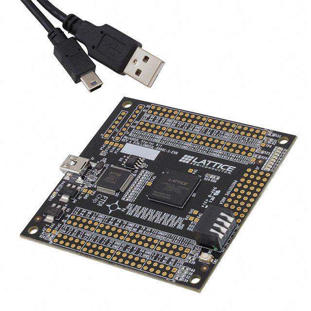
产品属性
| 类型 | 描述 | 全选 |
|---|---|---|
| 系列 | ECP3 | |
| 包装 | 散装 | |
| 产品状态 | 停止提供 | |
| 类型 | FPGA | |
| 配套使用/相关产品 | LFE3-95 | |
| 平台 | ECP3 FPGA 视频 | |
| 内含物 | 板 |
博客
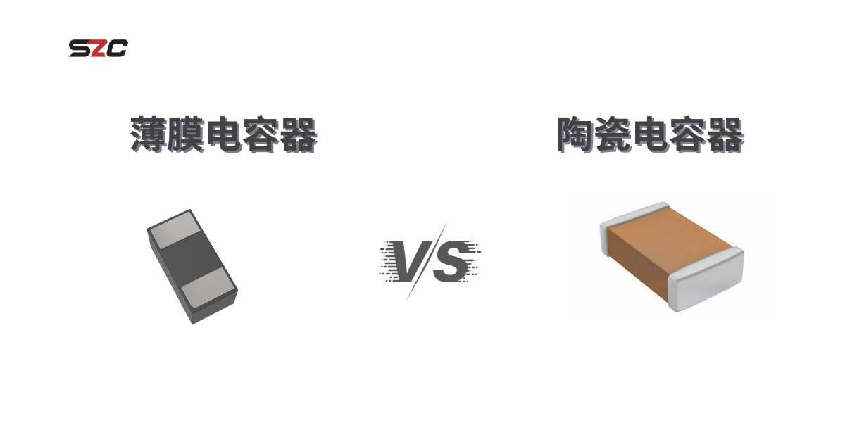
 深入探讨全球陶瓷电容器市场加入我们,一起探索全球陶瓷电容器市场中的最新趋势。
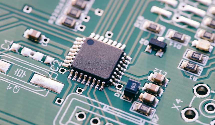 掌握使用微控制器进行电流测量与与模数转换器 (ADC) 顺利配合的电压不同,电流测量增加了一层复杂性,可能导致不准确。对当前测量细微差别的探索将揭示这些误差的根源,并引入超级英雄解决方案:片上模拟核心独立外设 (CIP)。
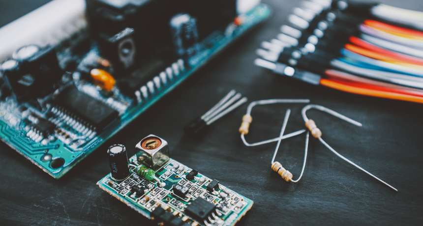
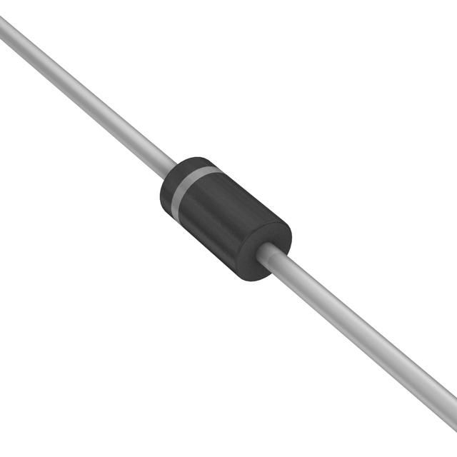 什么是整流二极管:初学者指南揭开整流二极管的秘密!链接整流二极管的定义,应用领域,工作原理,以及常见的整流二极管。
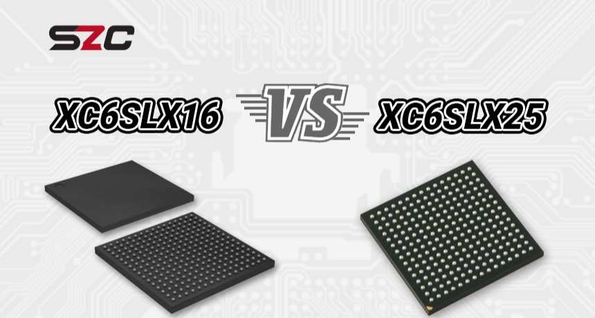 FPGA对比:XC6SLX16 vs. XC6SLX25通过我们的快速指南解锁fpga的秘密!XC6SLX16或xc6slx25 -哪一款是您下一次科技冒险的关键?点击现在探索可编程可能性的世界!
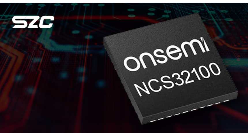
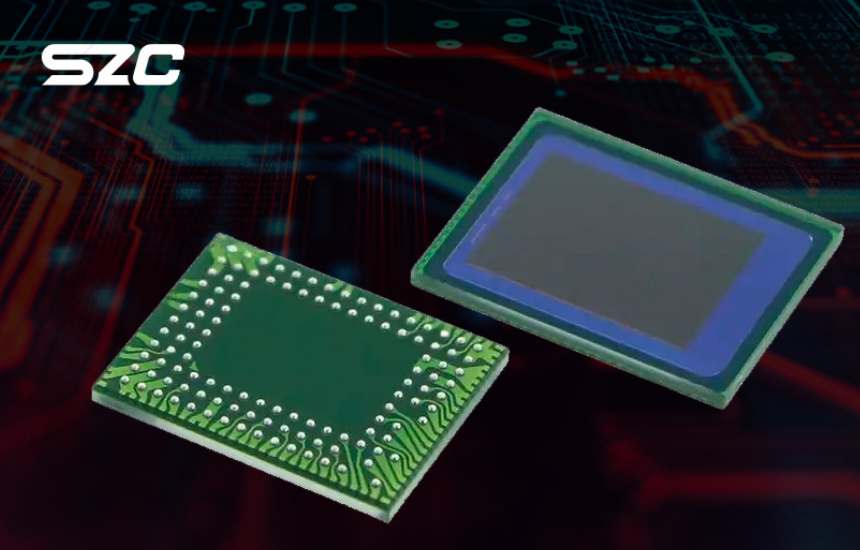 利用onsemi的先进图像传感器增强道路安全来看看onsemi的AR0220AT吧,它是高级驾驶辅助系统(Advanced Driver Assistance Systems)中的一款夜间智能游戏颠覆者。
面议
价格更新:一个月前
现货供应:
3574
Lattice Semiconductor Corporation
Lattice Semiconductor 是低功耗可编程的领导者。 在不断增长的通信、计算、工业、汽车和消费市场中,他们通过网络解决客户问题,从边缘到云端。 他们的技术、长期合作关系以及对世界级支持的承诺让他们的客户能够快速、轻松地释放他们的创新,以创造一个智能、安全和互联的世界。
查看所有产品从 Lattice Semiconductor Corporation博客
- 深入探讨全球陶瓷电容器市场加入我们,一起探索全球陶瓷电容器市场中的最新趋势。
- 掌握使用微控制器进行电流测量与与模数转换器 (ADC) 顺利配合的电压不同,电流测量增加了一层复杂性,可能导致不准确。对当前测量细微差别的探索将揭示这些误差的根源,并引入超级英雄解决方案:片上模拟核心独立外设 (CIP)。
- 什么是整流二极管:初学者指南揭开整流二极管的秘密!链接整流二极管的定义,应用领域,工作原理,以及常见的整流二极管。
- FPGA对比:XC6SLX16 vs. XC6SLX25通过我们的快速指南解锁fpga的秘密!XC6SLX16或xc6slx25 -哪一款是您下一次科技冒险的关键?点击现在探索可编程可能性的世界!
- 利用onsemi的先进图像传感器增强道路安全来看看onsemi的AR0220AT吧,它是高级驾驶辅助系统(Advanced Driver Assistance Systems)中的一款夜间智能游戏颠覆者。
热门制造商
View all manufactures 更多


热门产品
更多电子零件 更多
LFMXO5-25-EVN
DEV BOARD MACHXO5-NX W/FLASH
LCMXO3L-DSI-EVN
BOARD EVAL FOR MACHXO3L
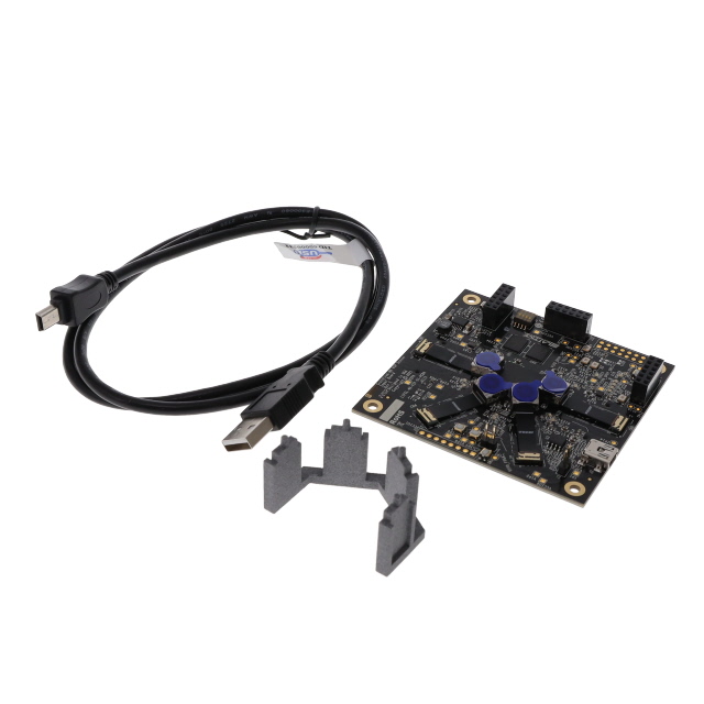
LFCPNX-VERSA-EVN
BOARD DEV CERTUSPRO-NX VERSA
LCMXO2-7000HE-B-EVN
BOARD BREAKOUT MACHX02
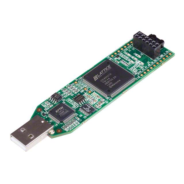
ICE5LP4K-B-EVN
BOARD EVAL FOR ICE5
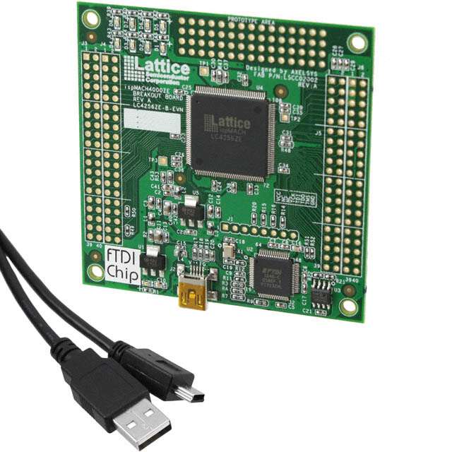
LC4256ZE-B-EVN
BOARD BREAKOUT ISPMACH 4256ZE
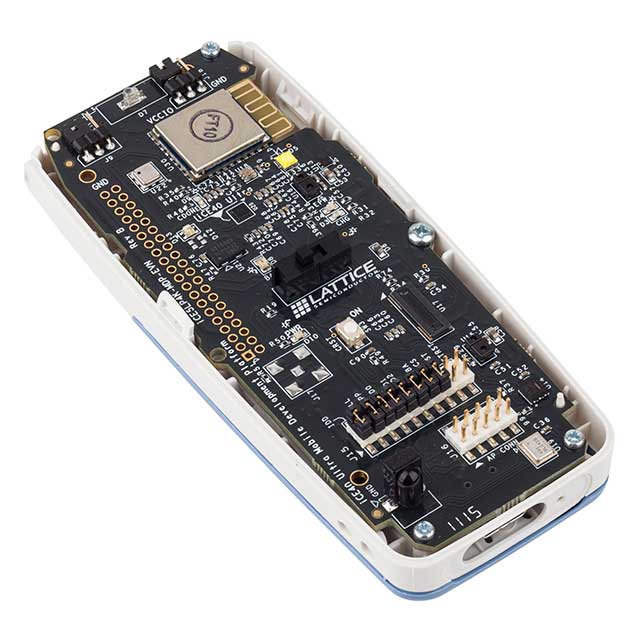
ICE5LP4K-MDP-EVN
DEV PLATFORM ICE40 ULTRA MOBILE
LIFCL-VIP-SI-EVN
BRD EV VIP SENS INPUT CRSLINK-NX
ICE40HX1K-STICK-EVN
BOARD EVAL FPGA ICESTICK
LCMXO3L-6900C-S-EVN
DEV KIT FOR MACHXO3L