


¥334.92
价格更新:一个月前
现货供应:
134


45
为45个国家的客户提供服务
1000+
全球制造商
$140M
5年增长1.4亿美元
50.0M+
5年内配送了5000万个元件
NXP USA Inc.
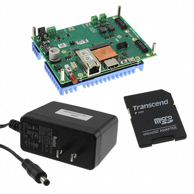
NXP Semiconductors 是嵌入式控制器的领先供应商,为包括汽车、无线连接等在内的各种行业提供范围广泛的 MCU 产品组合,这些 MCU 具有基于 Arm 的处理器和微控制器。 他们继续推动创新,为工业和汽车应用提供强大的电源管理产品组合,包括多种电源和电池管理解决方案。 恩智浦产品支持并连接全球构建解决方案,帮助提高人员、组织和整个世界的能力。 飞思卡尔半导体已被恩智浦半导体收购。 Freescale Semiconductor 部件现在是 NXP 系列的一部分(2015 年 12 月)。
查看所有产品从 NXP USA Inc.


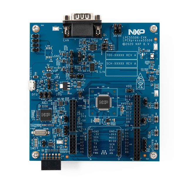
The LPC55S66JBD100K MCU family builds on the world’s first general-purpose Cortex-M33 based microcontroller introduced with the LPC5500 series. This high-efficiency family leverages the new Armv8-M architecture to introduce new levels of performance and advanced security capabilities including TrustZone-M and co-processor extensions. The LPC55S66JBD100K family enables these co-processors extensions and leverages them to bring significant signal processing efficiency gains from a proprietary DSP accelerator offering a 10x clock cycle reduction. An optional second Cortex-M33 core offers flexibility to balance high performance and power efficiency.
In addition, the LPC55S66JBD100K MCU family provides benefits from 40nm NVM based process technology cost advantages, broad scalable packages, and memory options, as well as a robust enablement including MCUXpresso Software and Tools ecosystem and low-cost development boards.
Feature
- Arm Cortex-M33 processor, running at a frequency of up to 150 MHz
- TrustZone, Floating Point Unit (FPU) and Memory Protection Unit (MPU)
- Arm Cortex-M33 built-in Nested Vectored Interrupt Controller (NVIC)
- Non-maskable Interrupt (NMI) input with a selection of sources
- Arm Cortex-M33 co-processor
- Running at a frequency of up to 100 MHz
- The configuration of this instance does not include MPU, FPU, DSP, ETM, and TrustZone
- System tick timer
- CASPER Crypto co-processor to enable hardware acceleration for certain asymmetric cryptographic algorithms
- PowerQuad hardware accelerator for (fixed and floating point) DSP functions
- Up to 640 KB on-chip flash program memory with a flash accelerator and 256-byte page erase and write
- Up to 320 KB total SRAM consisting of 288 KB on the system bus and 32 KB on Core Bus
- Arm TrustZone enabled
- PRINCE module for real-time encryption of data being written to on-chip flash and decryption of encrypted flash data during reading to allow asset protection
- AES-256 encryption/decryption engine
- Secure Hash Algorithm (SHA2) module supporting secure boot with dedicated DMA controller
- Physical Unclonable Function(PUF) using dedicated SRAM for silicon fingerprint. PUF can generate, store, and reconstruct key sizes from 64 to 4096 bits. Includes hardware for key extraction
- Random Number Generator (RNG)
- 128-bit unique device serial number for identification (UUID)
- Secure GPIO
- Flexcomm Interface contains up to nine serial peripherals. Each Flexcomm Interface can be selected by software to be a USART, SPI, I2C, and I2S interface
- I2C-bus interfaces support Fast-mode and Fast-mode Plus with data rates of up to 1Mbit/s and with multiple address recognition and monitor mode
- USB 2.0 full speed host/device controller with on-chip PHY and dedicated DMA controller supporting crystal-less operation in device mode
- USB 2.0 high-speed host/device controller with on-chip high-speed PHY
- DMA0 controller with 23 channels and up to 22 programmable triggers, able to access all memories and DMA-capable peripherals.
- DMA1 controller with 10 channels and up to 16 programmable triggers, able to access all memories and DMA-capable peripherals
- Secured digital input/output (SD/MMC and SDIO) card interface with DMA support. SDIO with support for up to two cards. Supported card types are MMC, SDIO, and CE-ATA. Supports SD2.0, and SR25
- CRC engine block can calculate a CRC on supplied data using one of three standard polynomials with DMA support.
- Up to 64 General-Purpose Input/Output (GPIO) pins.
- GPIO registers are located on the AHB for fast access. The DMA supports GPIO ports.
- Up to eight GPIOs can be selected as Pin Interrupts (PINT), triggered by rising, falling or both input edges.
- Two GPIO Grouped Interrupts (GINT) enable an interrupt based on a logical (AND/OR) combination of input states.
- I/O pin configuration with support for up to 16 function options.
- Programmable Logic Unit (PLU) to create small combinational and/or sequential logic networks including state machines
- 16-bit ADC with five differential channel pair (or 10 singled-ended channels), and with multiple internal and external trigger inputs and sample rates of up to 1.0MSamples/sec. The ADC supports two independent conversion sequences
- Integrated temperature sensor connected to the ADC
- Comparator with five input pins and external or internal reference voltage
- Five 32-bit standard general purpose asynchronous timers/counters, which support up to four capture inputs and four compare outputs. Specific timer events can be selected to generate DMA requests
- One SCTimer/PWM with eight input and ten output functions (including capture and match). Inputs and outputs can be routed to or from external pins and internally to or from selected peripherals. Internally, the SCTimer/PWM supports 16 match/captures, 16 events, and 32 states
- 32-bit Real-time clock (RTC) with 1 s resolution running in the always-on power domain. A timer in the RTC can be used for wake-up from all low power modes including deep power-down, with 1 ms resolution
- Multiple-channel multi-rate 24-bit timer (MRT) for repetitive interrupt generation at up to four programmable, fixed rates
- Windowed Watchdog Timer (WWDT) with FRO 1 MHZ as a clock source
- Micro-Tick Timer running from the watchdog oscillator can be sued to wake-up the device from sleep and deep-sleep modes
- 42-bit free running OS Timer as continuous time-base for the system, available in any reduced power modes.
- Internal Free Running Oscillator (FRO). This oscillator provides a selectable 96 MHz output, and a 12 MHz output (divided down from the selected higher frequency) that can be used as a system clock. The FRO is trimmed to +/- 1% accuracy over the entire voltage and temperature range
- 32 kHz Internal Free Running Oscillator FRO. The FRO is trimmed to +/- 1% accuracy over the entire voltage and temperature range
- Internal low power oscillator (FRO 1 MHz)
- Crystal oscillator with an operating frequency of 1 MHz to 25 MHz. Option for external clock input (bypass mode) for clock frequencies of up to 25 MHz
- Crystal oscillator with 32.768 kHz operating frequency
- PLL0 and LLL1 allows CPU operation up to the maximum CPU rate without the need for a high-frequency external clock
- Clock output function with divider to monitor internal clocks
- Frequency measurement unit for measuring the frequency of any on-chip or off-chip clock signal
- Integrated Power Management Unit (PMU) to minimize power consumption
- Reduced power modes: Sleep, deep-sleep with RAM retention, power-down with RAM retention and CPU0 retention, and deep power-down
- Configurable wake-up options from peripheral interrupts
- The Micro-Tick Timer running from the watchdog oscillator, and the Real-Time Clock (RTC) running from the 32.678 kHz clock, can be used to wake-up the device from sleep and deep-sleep modes
- Power-On Reset (POR)
- Brown-Out-Detect (BOD) with separate thresholds for interrupt and forced reset
- Operating from an internal DC-DC converter
- Single power supply 1.8V to 3.6V
- JTAG boundary scan supported
- Operating temperature range -40 °C to +105 °C
- Available in HLQFP100, VFBGA98, and HTQFP64 packages


相关产品
| 制造商零件编号 | 价格(¥) | 现有数量 | |
|---|---|---|---|
 LPC43S57JET256EIC MCU 32BIT 1MB FLASH 256LBGA | 225.00 |
4722
市场 | |
 LPC54608J512BD208EIC MCU 32BIT 512KB FLASH 208LQFP | 110.00 |
28
市场 | |
 LPC54018J2MET180ELPC54018 - ARM Cortex-M4, Bosch | 388.00 |
169
市场 | |
 LPC54018J2MET180EIC MCU 32BIT 2MB FLASH 180TFBGA | 87.27 |
2945
市场 | |
LPC54628J512ET180EIC MCU 32BIT 512KB FLSH 180TFBGA | 80.00 |
2352
市场 | |
 LPC54606J512BD100EIC MCU 32BIT 512KB FLASH 100LQFP | 18.00 |
3000
市场 | |
 LPC54113J256BD64QLIC MCU 32BIT 256KB FLASH 64LQFP | 30.00 |
2400
市场 |
-
LPC43S57JET256E
IC MCU 32BIT 1MB FLASH 256LBGA
-
LPC54608J512BD208E
IC MCU 32BIT 512KB FLASH 208LQFP
-
LPC54018J2MET180E
LPC54018 - ARM Cortex-M4, Bosch
-
LPC54018J2MET180E
IC MCU 32BIT 2MB FLASH 180TFBGA
-
LPC54628J512ET180E
IC MCU 32BIT 512KB FLSH 180TFBGA
-
LPC54606J512BD100E
IC MCU 32BIT 512KB FLASH 100LQFP
-
LPC54113J256BD64QL
IC MCU 32BIT 256KB FLASH 64LQFP
产品属性
| 类型 | 描述 | 全选 |
|---|---|---|
| 产品状态 | 在售 | |
| 类型 | MCU | |
| 核心处理器 | ARM® Cortex®-M33 | |
| 平台 | LPCXpresso™ | |
| 使用的 IC/零件 | LPC55S06 | |
| 安装类型 | 固定 | |
| 内含物 | 板 | |
| 系列 | LPC5500 | |
| 包装 | 散装 |
博客
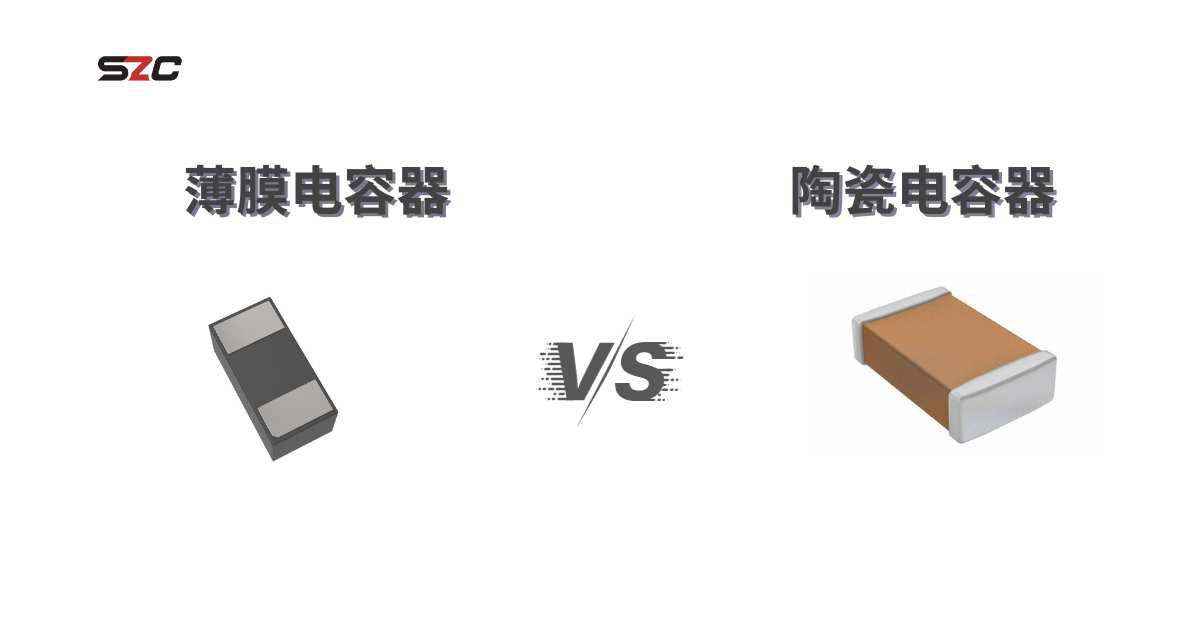
 深入探讨全球陶瓷电容器市场加入我们,一起探索全球陶瓷电容器市场中的最新趋势。
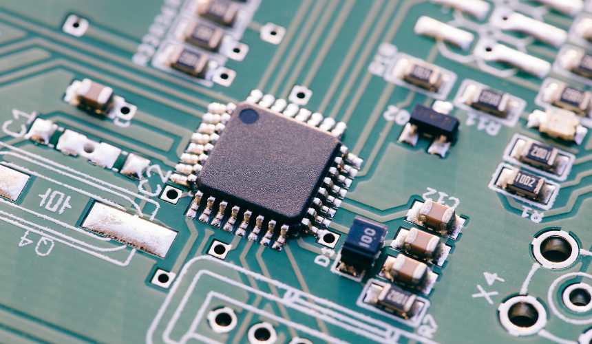 掌握使用微控制器进行电流测量与与模数转换器 (ADC) 顺利配合的电压不同,电流测量增加了一层复杂性,可能导致不准确。对当前测量细微差别的探索将揭示这些误差的根源,并引入超级英雄解决方案:片上模拟核心独立外设 (CIP)。
 什么是整流二极管:初学者指南揭开整流二极管的秘密!链接整流二极管的定义,应用领域,工作原理,以及常见的整流二极管。
 FPGA对比:XC6SLX16 vs. XC6SLX25通过我们的快速指南解锁fpga的秘密!XC6SLX16或xc6slx25 -哪一款是您下一次科技冒险的关键?点击现在探索可编程可能性的世界!
 利用onsemi的先进图像传感器增强道路安全来看看onsemi的AR0220AT吧,它是高级驾驶辅助系统(Advanced Driver Assistance Systems)中的一款夜间智能游戏颠覆者。

¥334.92
价格更新:一个月前
现货供应:
134
NXP USA Inc.
NXP Semiconductors 是嵌入式控制器的领先供应商,为包括汽车、无线连接等在内的各种行业提供范围广泛的 MCU 产品组合,这些 MCU 具有基于 Arm 的处理器和微控制器。 他们继续推动创新,为工业和汽车应用提供强大的电源管理产品组合,包括多种电源和电池管理解决方案。 恩智浦产品支持并连接全球构建解决方案,帮助提高人员、组织和整个世界的能力。 飞思卡尔半导体已被恩智浦半导体收购。 Freescale Semiconductor 部件现在是 NXP 系列的一部分(2015 年 12 月)。
查看所有产品从 NXP USA Inc.博客
- 深入探讨全球陶瓷电容器市场加入我们,一起探索全球陶瓷电容器市场中的最新趋势。
- 掌握使用微控制器进行电流测量与与模数转换器 (ADC) 顺利配合的电压不同,电流测量增加了一层复杂性,可能导致不准确。对当前测量细微差别的探索将揭示这些误差的根源,并引入超级英雄解决方案:片上模拟核心独立外设 (CIP)。
- 什么是整流二极管:初学者指南揭开整流二极管的秘密!链接整流二极管的定义,应用领域,工作原理,以及常见的整流二极管。
- FPGA对比:XC6SLX16 vs. XC6SLX25通过我们的快速指南解锁fpga的秘密!XC6SLX16或xc6slx25 -哪一款是您下一次科技冒险的关键?点击现在探索可编程可能性的世界!
- 利用onsemi的先进图像传感器增强道路安全来看看onsemi的AR0220AT吧,它是高级驾驶辅助系统(Advanced Driver Assistance Systems)中的一款夜间智能游戏颠覆者。
热门制造商
View all manufactures 更多


热门产品
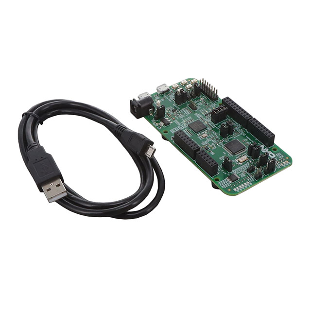
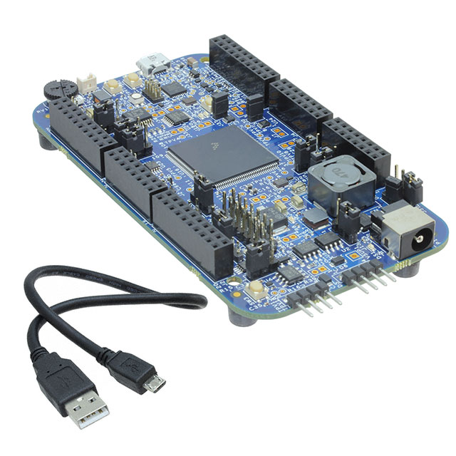
更多电子零件 更多LPC55S06-EVK
EVAL KIT LPC55
MC56F80000-EVK
DIGITAL SIGNAL CTRL EVAL KIT
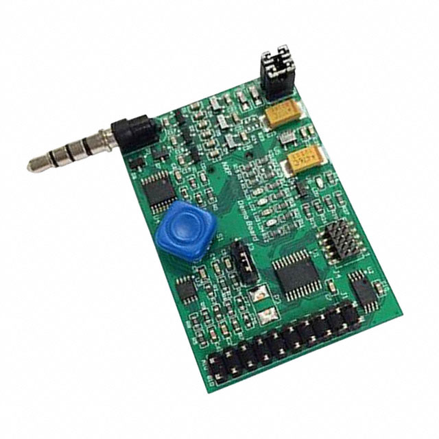
OM13069UL
SMARTPHONE QUICK-JACK SOL LPC812
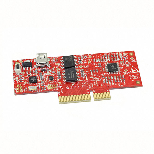
HVP-KV10Z32
HIGH-VOLTAGE DEV PLATFORM KV1X
MPC5744P-144DS
MPC5744P EVAL BRD
DEVKIT-MPC5748G
MPC5748G EVAL BRD
SBC-S32V234
S32V234 EVAL BRD
DEVKIT-MPC5744P
MPC5744P EVAL BRD
DEVKIT-S12VRP
S12VRP EVAL BRD
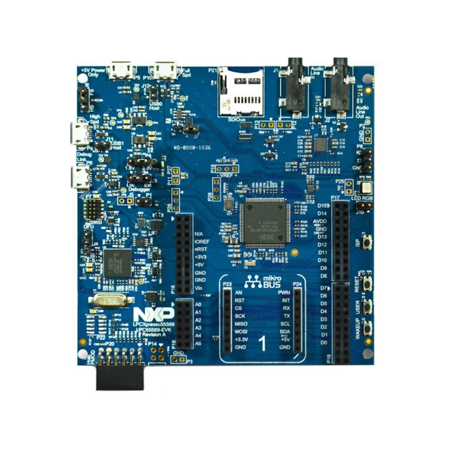
LPC55S69-EVK
LPCXPRESSO LPC55S6X EVAL BRD