


¥10.00
价格更新:一个月前
现货供应:
200


45
为45个国家的客户提供服务
1000+
全球制造商
$140M
5年增长1.4亿美元
50.0M+
5年内配送了5000万个元件

Renesas Electronics America Inc.
Renesas Electronics Corporation 通过完整的半导体解决方案提供值得信赖的嵌入式设计创新,使数十亿互联的智能设备能够改善人们安全可靠的工作和生活方式。 作为微控制器、模拟、电源和 SoC 产品及集成平台的全球领导者,瑞萨为广泛的汽车、工业、家用电子、办公自动化和信息通信技术应用提供专业知识、质量和全面的解决方案,以帮助塑造一个 无限的未来。
查看所有产品从 Renesas Electronics America Inc.


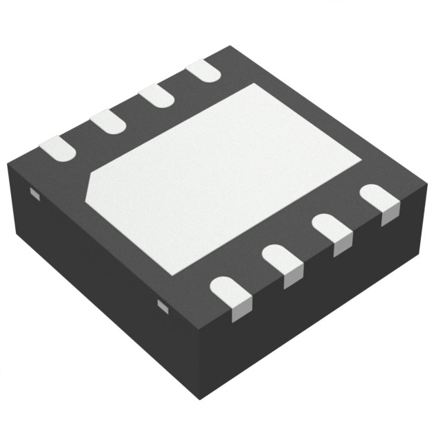
Low Voltage ORing FET Controller The ISL6146AFRZ represents a family of ORing MOSFET controllers capable of ORing voltages from 1V to 18V. Together with suitably sized N-channel power MOSFETs, the ISL6146AFRZ increases power distribution efficiency when replacing a power ORing diode in high current applications. It provides gate drive voltage for the MOSFET(s) with a fully integrated charge pump.
The ISL6146AFRZ represents a family of ORing MOSFET controllers capable of ORing voltages from to 18V. Together with suitably sized N-channel power MOSFETs, the ISL6146AFRZ increases power distribution efficiency when replacing a power ORing diode in high current applications. It provides gate drive voltage for the MOSFET(s) with a fully integrated charge pump. The ISL6146AFRZ allows users to adjust with external resistor(s) the VOUT - VIN trip point, which adjusts the control sensitivity to system power supply noise. An open drain FAULT pin will indicate if a conditional or FET fault has occurred. The ISL6146A and ISL6146B are optimized for very low voltage operation, down to 1V with an additional independent bias 3V or greater. The ISL6146C provides a voltage compliant mode of operation down to 3V with programmable Undervoltage Lock Out and Overvoltage Protection threshold levels.
TABLE 1. KEY DIFFERENCES BETWEEN PARTS IN FAMILY PART NUMBER ISL6146B ISL6146C KEY DIFFERENCES Separate BIAS and VIN with Active High Enable Separate BIAS and VIN with Active Low Enable VIN with OVP/UVLO Inputs
FeaturesORing Down to 1V and to 20V with ISL6146A, ISL6146B Programmable Voltage Compliant Operation with ISL6146C VIN Hot Swap Transient Protection Rating to +24V High Speed Comparator Provides Fast <0.3�s Turn-off in Response to Shorts on Sourcing Supply. Fastest Reverse Current Fault Isolation with 6A Turn-off Current Very Smooth Switching Transition Internal Charge Pump to Drive N-channel MOSFET User Programmable VIN - VOUT Vth for Noise Immunity Open Drain FAULT Output with Delay - Short between any two of the ORing FET Terminals - GATE Voltage and Excessive FET VDS - Power-Good Indicator (ISL6146C) MSOP and DFN Package Options
ApplicationsN+1 Industrial and Telecom Power Distribution Systems Uninterruptable Power Supplies Low Voltage Processor and Memory Storage and Datacom Systems
Q1 + VIN GATE VOUT BIAS ADJ ISL6146B FLT GND Q2 + VIN GATE VOUT BIAS ADJ ISL6146B FLT GND EN+C GATE FAST OFF, ~200ns FALL TIME ~70ns FROM TO 12.6V ACROSS 57nF GATE OUTPUT SINKING ~ 6A
CAUTION: These devices are sensitive to electrostatic discharge; follow proper IC Handling Procedures. 1-888-468-3774 | Copyright Intersil Americas Inc. 2011. All Rights Reserved Intersil (and design) is a trademark owned by Intersil Corporation or one of its subsidiaries. All other trademarks mentioned are the property of their respective owners.
BIAS Q-PUMP VDS FORWARD REGULATOR GATE FAULT DIAGNOSTIC 1. VIN - VOUT 570mV 2. GATE - VIN 220mV 3. TEMP +150�C 4. VBIAS < POR (ISL6146A/B) 5. VIN OR VOUT < POR (ISL6146C) 6. VIN < VOUT UVLO 8mA ENABLE EN/EN ENABLE EN + FLT
MSOP/ DFN 1 SYMBOL GATE DESCRIPTION Gate Drive output to the external N-Channel MOSFET generated by the IC internal charge pump. Gate turn-on time is typically <1ms. Allows active control of external N-Channel FET gate to perform ORing function. The GATE drive is between VIN 7V at VIN = 3.3V and VIN +12V at VIN = 18V. Connected to the sourcing supply side (ORing MOSFET Source), this pin serves as the sense pin to determine the OR'd supply voltage. The ORing MOSFET will be turned off when VIN becomes lower than VOUT by a value more than the externally set threshold or the defaulted internal threshold. Range: to 24V Primary bias pin. Connected to an independent voltage supply greater than or equal to 3V and greater than VIN. Range: to 24V Programmable UVLO protection to prevent premature turn-on prior to VIN being adequately biased. Range: to 24V Active high enable input to turn on the FET. Internally pulled low to GND through 2M Range: to 24V Active low enable input to turn on the FET. Internally pulled high to BIAS through 2M. Range: to 24V
MSOP/ DFN 5 6 SYMBOL OVP GND FAULT (Continued) DESCRIPTION Programmable OV protection to prevent continued operation when the monitored voltage is too high. A back-to-back FET configuration must be employed to implement the OVP capability. Range: to 24V Chip ground reference. Open-Drain pull-down fault indicating output with internal on chip filtering (TFLT). The ISL6146AFRZ fault detection circuitry will pull-down this pin to GND as it detects a fault to a disable input. Different types of faults and their detection mechanisms are discussed in more detail on page 16, these faults include: a. GATE is OFF (GATE < VIN or b. VIN-VOUT > 0.57V when ON. c. FET G-D or G-S or D-S shorts. d. VIN PORL2H e. VIN < VOUT f. Over-Temperature Range: 0 to VOUT Resistor programmable VIN - VOUT Voltage Threshold (Vth) of the High Speed Comparator. This pin is either directly connected to VOUT or can be connected through to 100k resistor to GND. Allows for adjusting the voltage difference threshold to prevent unintended turn-off of the pass FET due to normal system voltage fluctuations. Range: 0.4 to VOUT The second sensing node for external FET control and connected to the Load side (ORing MOSFET Drain). This is the common connection point for multiple paralleled supplies. VOUT is compared to VIN to determine when the ORing FET has to be turned off. Range: to 24V Connect to GND
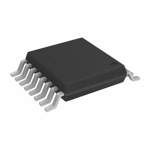
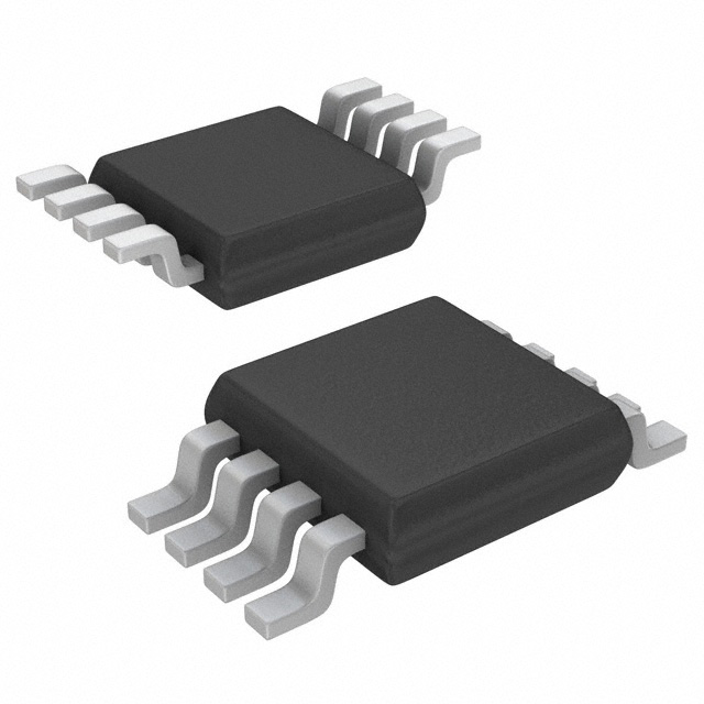
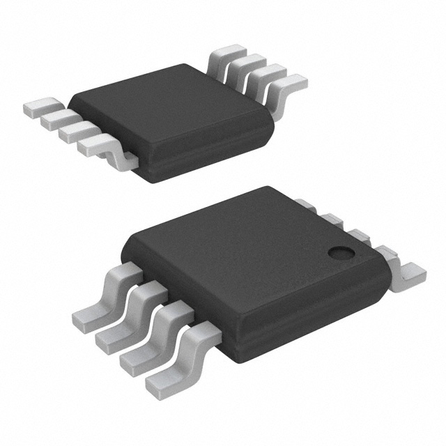
PART NUMBER (Notes 3) ISL6146AFUZ (Note ISL6146AFRZ ISL6146BFUZ (Note ISL6146BFRZ ISL6146CFUZ (Note ISL6146BEVAL1Z ISL6146CEVAL1Z NOTES: 1. Add "-T*" suffix for tape and reel. Please refer to TB347 for details on reel specifications. 2. These Intersil Pb-free plastic packaged products employ special Pb-free material sets, molding compounds/die attach materials, and 100% matte tin plate plus anneal (e3 termination finish, which is RoHS compliant and compatible with both SnPb and Pb-free soldering operations). Intersil Pb-free products are MSL classified at Pb-free peak reflow temperatures that meet or exceed the Pb-free requirements of IPC/JEDEC STD-020. 3. For Moisture Sensitivity Level (MSL), please see device information page for ISL6146. For more information on MSL please see techbrief TB363. 4. MSOP packaged parts to be released soon. PART MARKING 6146C 46CF TEMP RANGE (�C) 8 Ld MSOP Ld 3x3 DFN 8 Ld MSOP Ld 3x3 DFN 8 Ld MSOP Ld 3x3 DFN PACKAGE (Pb-free) PKG. DWG. M8.118 L8.3x3J
ISL6146A Evaluation Board ISL6146B Evaluation Board ISL6146B Evaluation BoardFeature
- OR-ing down to 1V and up to 20V with ISL6146A, ISL6146B, ISL6146D and ISL6146E
- Programmable voltage compliant operation with ISL6146C
- VIN hot swap transient protection rating to +24V
- High speed comparator provides fast <0.3µs turn-off in response to shorts on sourcing supply
- Fastest reverse current fault isolation with 6A turn-off current
- Very smooth switching transition
- Internal charge pump to drive N-channel MOSFET
- User programmable VIN - VOUT Vth for noise immunity
- Open-drain FAULT output with delay - Short between any two of the OR-ing FET terminals
- GATE voltage and excessive FET VDS
- Power-good indicator (ISL6146C)
- MSOP and DFN package options


产品属性
| 类型 | 描述 | 全选 |
|---|---|---|
| 电流 - 供电 | 25 µA | |
| 延迟时间 - 关闭 | 65 ns | |
| 内部开关 | 无 | |
| 比率 - 输入:输出 | N:1 | |
| 供应商器件封装 | 8-DFN(3x3) | |
| 封装/外壳 | 8-VDFN 裸露焊盘 | |
| FET 类型 | N 通道 | |
| 类型 | N+1 ORing 控制器 | |
| 安装类型 | 表面贴装型 | |
| 产品状态 | 停产 | |
| 工作温度 | -40°C ~ 125°C | |
| 包装 | 管件 | |
| 应用 | N+1 电源,电信/数据通信系统 | |
| 电压 - 供电 | 3V ~ 20V |
博客

 深入探讨全球陶瓷电容器市场加入我们,一起探索全球陶瓷电容器市场中的最新趋势。
 掌握使用微控制器进行电流测量与与模数转换器 (ADC) 顺利配合的电压不同,电流测量增加了一层复杂性,可能导致不准确。对当前测量细微差别的探索将揭示这些误差的根源,并引入超级英雄解决方案:片上模拟核心独立外设 (CIP)。
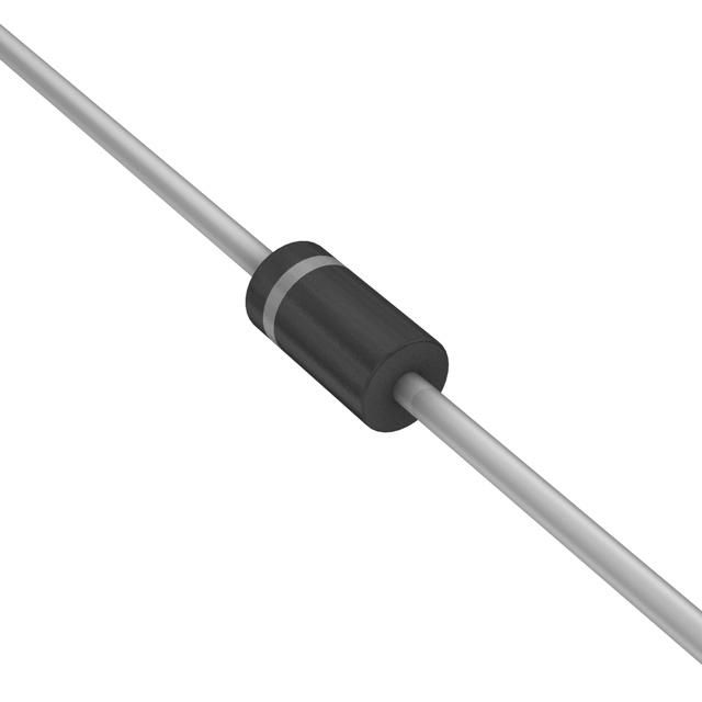 什么是整流二极管:初学者指南揭开整流二极管的秘密!链接整流二极管的定义,应用领域,工作原理,以及常见的整流二极管。
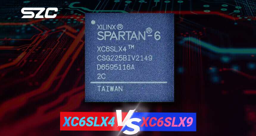
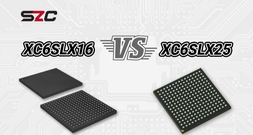 FPGA对比:XC6SLX16 vs. XC6SLX25通过我们的快速指南解锁fpga的秘密!XC6SLX16或xc6slx25 -哪一款是您下一次科技冒险的关键?点击现在探索可编程可能性的世界!
 利用onsemi的先进图像传感器增强道路安全来看看onsemi的AR0220AT吧,它是高级驾驶辅助系统(Advanced Driver Assistance Systems)中的一款夜间智能游戏颠覆者。


¥10.00
价格更新:一个月前
现货供应:
200
Renesas Electronics America Inc.
Renesas Electronics Corporation 通过完整的半导体解决方案提供值得信赖的嵌入式设计创新,使数十亿互联的智能设备能够改善人们安全可靠的工作和生活方式。 作为微控制器、模拟、电源和 SoC 产品及集成平台的全球领导者,瑞萨为广泛的汽车、工业、家用电子、办公自动化和信息通信技术应用提供专业知识、质量和全面的解决方案,以帮助塑造一个 无限的未来。
查看所有产品从 Renesas Electronics America Inc.博客
- 深入探讨全球陶瓷电容器市场加入我们,一起探索全球陶瓷电容器市场中的最新趋势。
- 掌握使用微控制器进行电流测量与与模数转换器 (ADC) 顺利配合的电压不同,电流测量增加了一层复杂性,可能导致不准确。对当前测量细微差别的探索将揭示这些误差的根源,并引入超级英雄解决方案:片上模拟核心独立外设 (CIP)。
- 什么是整流二极管:初学者指南揭开整流二极管的秘密!链接整流二极管的定义,应用领域,工作原理,以及常见的整流二极管。
- FPGA对比:XC6SLX16 vs. XC6SLX25通过我们的快速指南解锁fpga的秘密!XC6SLX16或xc6slx25 -哪一款是您下一次科技冒险的关键?点击现在探索可编程可能性的世界!
- 利用onsemi的先进图像传感器增强道路安全来看看onsemi的AR0220AT吧,它是高级驾驶辅助系统(Advanced Driver Assistance Systems)中的一款夜间智能游戏颠覆者。
热门制造商
View all manufactures 更多


热门产品
更多电子零件 更多ISL6146AFRZ
IC OR CTRLR N+1 8DFN
ISL6146BFRZ-TK
IC OR CTRLR N+1 8DFN
ISL6146BFRZ-T
IC OR CTRLR N+1 8DFN
ISL6144IVZA
IC OR CTRLR N+1 16TSSOP
ISL6146AFUZ-TK
IC OR CTRLR N+1 8MSOP
ISL6146AFUZ-T
IC OR CTRLR N+1 8MSOP
ISL6146BFRZ
IC OR CTRLR N+1 8DFN
ISL6146AFUZ-T7A
IC OR CTRLR N+1 8MSOP
ISL6144IR
BUFFER/INVERTER MOSFET DRIVER
ISL6146BFRZ-T7A
IC OR CTRLR N+1 8DFN