All categories
- All categories
- Integrated Circuits (ICs)
- Development Boards, Kits, Programmers
- Discrete Semiconductor Products
- Power Supplies - Board Mount
- RF and Wireless
- Sensors, Transducers
- Memory Cards, Modules
- Audio Products
- Circuit Protection
- Crystals, Oscillators, Resonators
- Filters
- Isolators
- Kits
- Maker/DIY, Educational
- Optoelectronics
- Power Supplies - External/Internal (Off-Board)
- Relays
- Resistors
- Test and Measurement
- Uncategorized
- Inductors, Coils, Chokes
- Motors, Actuators, Solenoids and Drivers
- Switches
- Embedded Computers
- Capacitors
- Transformers
- Battery Products
- Products
- All categories
-
Integrated Circuits (ICs)
-
Embedded
- FPGAs (Field Programmable Gate Array)
- Microcontrollers
- CPLDs (Complex Programmable Logic Devices)
- FPGAs (Field Programmable Gate Array) with Microcontrollers
- PLDs (Programmable Logic Device)
- Microcontrollers, Microprocessor, FPGA Modules
- System On Chip (SoC)
- Application Specific Microcontrollers
- DSP (Digital Signal Processors)
- Microprocessors
-
Interface
- Drivers, Receivers, Transceivers
- Sensor and Detector Interfaces
- Analog Switches - Special Purpose
- Analog Switches, Multiplexers, Demultiplexers
- CODECS
- Controllers Interface ICs
- Direct Digital Synthesis (DDS)
- Encoders, Decoders, Converters
- Filters - Active
- I/O Expanders
- Modems - ICs and Modules
- Modules
- Sensor, Capacitive Touch
- Signal Buffers, Repeaters, Splitters
- Signal Terminators
- Specialized
- Telecom
- Serializers, Deserializers
- UARTs (Universal Asynchronous Receiver Transmitter)
- Voice Record and Playback
- Memory
-
Power Management (PMIC)
- DC DC Switching Controllers
- Display Drivers
- Full Half-Bridge Drivers
- Gate Drivers
- LED Drivers
- Motor Drivers, Controllers
- Power Distribution Switches, Load Drivers
- Power Management - Specialized
- Power Supply Controllers, Monitors
- Special Purpose Regulators
- Supervisors
- Voltage Regulators - DC DC Switching Regulators
- Voltage Regulators - Linear
- Voltage Regulators - Linear + Switching
- AC DC Converters, Offline Switches
- Battery Chargers
- Battery Management
- Current Regulation/Management
- Energy Metering
- Hot Swap Controllers
- Laser Drivers
- Lighting, Ballast Controllers
- OR Controllers, Ideal Diodes
- PFC (Power Factor Correction)
- Power Over Ethernet (PoE) Controllers
- RMS to DC Converters
- Thermal Management
- Voltage Reference
- Voltage Regulators - Linear Regulator Controllers
- V/F and F/V Converters
- Specialized ICs
- Audio Special Purpose
- Clock/Timing
- Data Acquisition
- Linear
-
Logic
- Buffers, Drivers, Receivers, Transceivers
- Comparators
- FIFOs Memory
- Flip Flops
- Gates and Inverters
- Gates and Inverters - Multi-Function, Configurable
- Multivibrators
- Shift Registers
- Signal Switches, Multiplexers, Decoders
- Translators, Level Shifters
- Latches
- Specialty Logic
- Counters, Dividers
- Parity Generators and Checkers
- Universal Bus Functions
-
Embedded
-
Development Boards, Kits, Programmers
- Accessories
- Evaluation and Demonstration Boards and Kits
- Evaluation Boards - DC/DC & AC/DC (Off-Line) SMPS
- Evaluation Boards - Expansion Boards, Daughter Cards
- Evaluation Boards - LED Drivers
- Evaluation Boards - Sensors
- Evaluation Boards - Embedded - Complex Logic (FPGA, CPLD)
- Evaluation Boards - Embedded - MCU, DSP
- Programmers, Emulators, and Debuggers
- Software, Services
- Evaluation Boards - Analog to Digital Converters (ADCs)
- Evaluation Boards - Audio Amplifiers
- Evaluation Boards - Digital to Analog Converters (DACs)
- Evaluation Boards - Linear Voltage Regulators
- Evaluation Boards - Op Amps
- Programming Adapters, Sockets
- RF Evaluation and Development Kits, Boards
- RFID Evaluation and Development Kits, Boards
-
Discrete Semiconductor Products
- Power Supplies - Board Mount
-
RF and Wireless
- RF Amplifiers
- Attenuators
- RF Accessories
- RF Demodulators
- RF Detectors
- RF Front End (LNA + PA)
- RF Misc ICs and Modules
- RF Mixers
- RF Modulators
- RF Power Controller ICs
- RF Power Dividers/Splitters
- RF Receivers
- RF Shields
- RF Switches
- RF Transceiver ICs
- RF Transceiver Modules and Modems
- RF Transmitters
- RFID, RF Access, Monitoring ICs
- RFID Transponders, Tags
- RF Multiplexers
- RF Receiver, Transmitter, and Transceiver Finished Units
- RF Antennas
- RFI and EMI - Contacts, Fingerstock and Gaskets
- RFID Reader Modules
- RF Circulators and Isolators
- RF Directional Coupler
- Balun
- Subscriber Identification Module (SIM) Cards
- RFID Accessories
- RFID Antennas
-
Sensors, Transducers
- Current Sensors
- Magnetic Sensors
- Position Sensors
- Specialized Sensors
- Temperature Sensors
- Motion Sensors
- Multifunction
-
Optical Sensors
- Ambient Light, IR, UV Sensors
- Image Sensors, Camera
- Photodiodes
- Distance Measuring
- Photointerrupters - Slot Type - Transistor Output
- Phototransistors
- Reflective - Analog Output
- Reflective - Logic Output
- Photo Detectors - Logic Output
- Photointerrupters - Slot Type - Logic Output
- Photoelectric, Industrial
- Camera Modules
- Photo Detectors - Remote Receiver
- Sensor, Transducer Accessories
- Sensor, Transducer Amplifiers
- Color Sensors
- Encoders
- Encoders - Industrial
- Touch Sensors
- Pressure Sensors, Transducers
- Flow Sensors
- Gas Sensors
- Pressure Sensors, Transducers - Industrial
- Float, Level Sensors
- Magnets
- Proximity Sensors
- Flow Sensors - Industrial
- Humidity, Moisture Sensors
- Memory Cards, Modules
- Audio Products
- Circuit Protection
- Crystals, Oscillators, Resonators
- Filters
- Isolators
- Kits
- Maker/DIY, Educational
-
Optoelectronics
- Circuit Board Indicators, Arrays, Light Bars, Bar Graphs
- Fiber Optic Transceiver Modules
- LED Character and Numeric
- COBs, Engines, Modules, Strips
- Color LED Lighting
- Display Bezels, Lenses
- Fiber Optic Receivers
- Fiber Optic Transmitters - Discrete
- Fiber Optic Transmitters - Drive Circuitry Integrated
- Laser Diodes, Modules
- LED Dot Matrix and Cluster
- LED Emitters - Infrared, UV, Visible
- LED Indication - Discrete
- Lenses
- Optoelectronics Accessories
- White LED Lighting
- Incandescent, Neon Lamps
- Fiber Optic Switches, Multiplexers, Demultiplexers
- Ballasts, Inverters
- LCD, OLED, Graphic
- LCD, OLED Character and Numeric
- Display, Monitor - LCD Driver/Controller
- Power Supplies - External/Internal (Off-Board)
- Relays
- Resistors
- Test and Measurement
- Uncategorized
- Inductors, Coils, Chokes
- Motors, Actuators, Solenoids and Drivers
- Switches
- Embedded Computers
- Capacitors
- Transformers
- Battery Products
- Manufacturers
- Services
- Industries
- Top-Quality Commitment
- Resources
SSTUG32866EC/G,518 datasheet
SSTUG32866EC/G,518 pdf
SSTUG32866EC/G,518 distributor
SSTUG32866EC/G,518 manufacturer
SSTUG32866EC/G,518 supplier
SSTUG32866EC/G,518 price
SSTUG32866EC/G,518 specification
SSTUG32866EC/G,518 wholesale
SSTUG32866EC/G,518 package
SSTUG32866EC/G,518 NXP USA Inc.
SSTUG32866EC/G,518
Compare
SSTUG32866EC/G,518
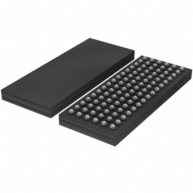
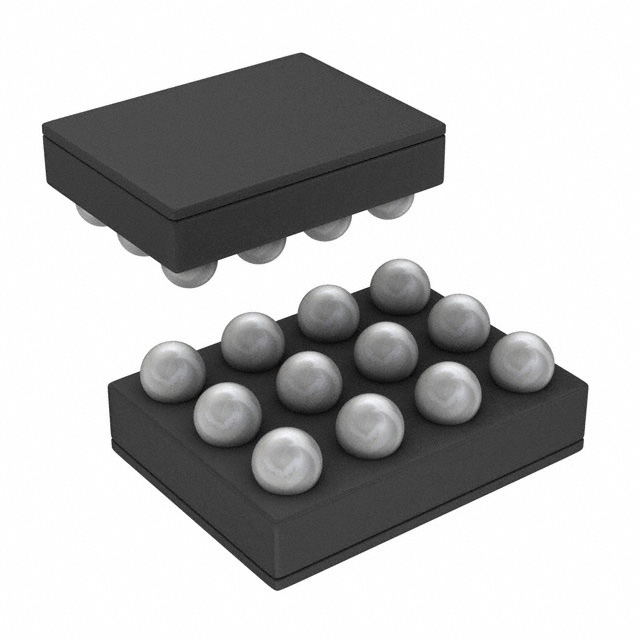
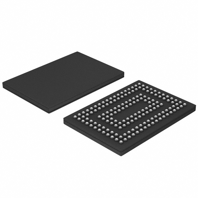
IC BUFFER 1.8V 25BIT 96-LFBGA
Compare
Obsolete
Quantity Available:
3756
SZC Quality Assurance


NXP USA Inc.
NXP Semiconductors, a frontrunner in embedded controllers, offers a wide array of MCUs with Arm-based processors. Their innovation extends to robust Power Management for industry and automotive use. NXP's products globally empower and interconnect, fostering proficiency for individuals, organizations, and the world. Noteworthy is the integration of Freescale Semiconductor into NXP (December 2015).
View All Product from NXP USA Inc.Popular Products
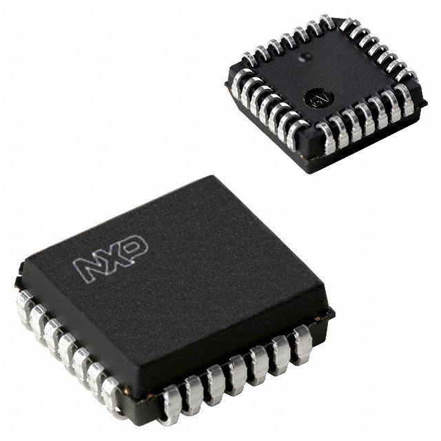
 GTL2002DP,118IC TRANSLTR BIDIRECTIONAL 8TSSOPObsolete Detail
 TEF8231EN1/N1ZZFULLY INTEGRATED 77 GHZ RFCMOS A$22.90 Detail
 PHM12NQ20T,518MOSFET N-CH 200V 14.4A 8HVSONObsolete Detail
- MC33FS8520A0ESR2SAFETY POWER MANAGEMENT IC, QFN5$6.04 Detail
 MC88915TFN160IC CLOCK DRIVER 28PLCCObsolete Detail
Product Details
Shipping
Quality Guarantee
Reviews
SSTUG32866EC/G,518 2. Features
The SSTUG32866 is a 1.8 V configurable register specifically designed for use on DDR2memory modules requiring a parity checking function. It is defined in accordance with theJEDEC standard for the SSTUG32866 registered buffer. The register is configurable(using configuration pins C0 and C1) to two topologies: 25-bit 1 : 1 or 14-bit 1 : 2, and inthe latter configuration can be designated as Register A or Register B on the DIMM.The SSTUG32866 accepts a parity bit from the memory controller on its parity bit(PAR_IN) input, compares it with the data received on the DIMM-independent D-inputsand indicates whether a parity error has occurred on its open-drain QERR pin(active LOW). The convention is even parity, that is, valid parity is defined as an evennumber of ones across the DIMM-independent data inputs combined with the parity inputbit.The SSTUG32866 is packaged in a 96-ball, 6 · 16 grid, 0.8 mm ball pitch LFBGApackage (13.5 mm · 5.5 mm).n Configurable register supporting DDR2 up to 800 MT/s Registered DIMM applicationsn Configurable to 25-bit 1 : 1 mode or 14-bit 1 : 2 moden Controlled output impedance drivers enable optimal signal integrity and speedn Meets or exceeds SSTUG32866 JEDEC standard speed performancen Supports up to 550 MHz clock frequency of operationn Optimized pinout for high-density DDR2 module designn Chip-selects minimize power consumption by gating data outputs from changing staten Supports SSTL_18 data inputsn Checks parity on the DIMM-independent data inputsn Partial parity output and input allows cascading of two SSTUG32866s for correct parityerror processingn Differential clock (CK and CK) inputsn Supports LVCMOS switching levels on the control and RESET inputsn Single 1.8 V supply operation (1.7 V to 2.0 V)n Available in 96-ball, 13.5 mm · 5.5 mm, 0.8 mm ball pitch LFBGA package
SSTUG32866EC/G,518 1. General description
SSTUG32866EC/G,518 with parity for DDR2-1G RDIMM applications
Rev. 01 — 29 June 2007Product data sheet
Shipping Cost
- 1. Shipping starts at $40, but prices may vary for certain countries like South Africa, Brazil, India, Pakistan, Israel, etc.
- 2. The basic freight for packages ≤0.5kg or equivalent volume is influenced by the time zone and country.
Shipping Method
- 1. Our products are currently shipped using DHL, SF, and UPS. For low quantities, FedEx is the chosen carrier.
Delivery Time
- 1. Once shipped, the estimated delivery time is contingent on the selected shipping method.
1. Every electronic component you purchase from us comes with a 365-Day Warranty. We stand behind the quality of our products.
2. Should you receive any item that isn't in perfect condition, we are committed to arranging a refund or replacement responsibly. Please note that items must be in their original condition for these options to be available.
FAQs:Q: How does SZComponents ensure that SSTUG32866EC/G,518 is genuinely manufactured or distributed by ?
A: Our professional business development department conducts rigorous testing and verification of the qualifications of original manufacturers and agents of . All suppliers must undergo and pass our qualification review before they are allowed to list their SSTUG32866EC/G,518 devices on our platform. We prioritize the sourcing channels and quality of SSTUG32866EC/G,518 products above everything else, ensuring thorough supplier audits so you can make your purchase with utmost confidence.
Q: Where can I find detailed information about SSTUG32866EC/G,518 chips, including original manufacturer details, Specialty Logic application, and images?
A: Utilize SZComponents's intelligent search engine, filter by the Specialty Logic category, or navigate through the 's brand page for comprehensive information.
Q: Are the prices and stock levels of 's SSTUG32866EC/G,518 shown on the platform accurate?
A: Due to significant fluctuations in 's inventory, real-time updates are challenging. However, we ensure periodic updates within 24 hours. We recommend confirming your SSTUG32866EC/G,518 order with a SZComponents sales representative or through our online customer service before proceeding with payment.
Q: What payment methods are accepted by SZComponents?
A: We accept various payment methods, including TT Bank, PayPal, Credit Card, Western Union, and Escrow.
Q: How are shipping arrangements made, and how can I track my package?
A: Customers can select from industry-leading freight companies like DHL, FedEx, UPS, TNT, and Registered Mail. Once your order is ready for shipment, our sales team will inform you about the shipping details and provide a tracking number. Note that tracking information might take up to 24 hours to appear. Typically, Express delivery takes 3-5 days, while Registered Mail requires 25-60 days.
Q: What is the process for returns or replacements of SSTUG32866EC/G,518?
A: We conduct a Pre-Shipment Inspection (PSI) on randomly selected batches from your order to ensure quality before shipment. We will accept returns or replacements of the SSTUG32866EC/G,518 if it does not meet your expectations under the following conditions:
- Issues such as incorrect quantities, delivery of wrong items, or obvious external defects are acknowledged by us.
- We are informed about the defects within 90 days from the delivery date.
- The SSTUG32866EC/G,518 remains unused and in its original packaging.
- To initiate a return, please:
- Inform us within the 90-day period.
- Obtain a Request for Return Authorization.
- For more details, refer to our Return & Change Policy.
Q: How can I get support or request datasheets and pin diagrams for SSTUG32866EC/G,518?
A: For any After-Sales service, including datasheets and pin diagrams for SSTUG32866EC/G,518, feel free to contact us at [email protected]
Q: How can I contact SZComponents? Please provide specific contact methods.
A: Reach out to us by clicking the customer service button at the bottom right corner of our site, submitting an RFQ directly, or using the 'Contact Us' link at the top of our page to email or call us. We guarantee a response to your inquiries within 24 hours.
Q: How does SZComponents ensure that SSTUG32866EC/G,518 is genuinely manufactured or distributed by ?
A: Our professional business development department conducts rigorous testing and verification of the qualifications of original manufacturers and agents of . All suppliers must undergo and pass our qualification review before they are allowed to list their SSTUG32866EC/G,518 devices on our platform. We prioritize the sourcing channels and quality of SSTUG32866EC/G,518 products above everything else, ensuring thorough supplier audits so you can make your purchase with utmost confidence.
Q: Where can I find detailed information about SSTUG32866EC/G,518 chips, including original manufacturer details, Specialty Logic application, and images?
A: Utilize SZComponents's intelligent search engine, filter by the Specialty Logic category, or navigate through the 's brand page for comprehensive information.
Q: Are the prices and stock levels of 's SSTUG32866EC/G,518 shown on the platform accurate?
A: Due to significant fluctuations in 's inventory, real-time updates are challenging. However, we ensure periodic updates within 24 hours. We recommend confirming your SSTUG32866EC/G,518 order with a SZComponents sales representative or through our online customer service before proceeding with payment.
Q: What payment methods are accepted by SZComponents?
A: We accept various payment methods, including TT Bank, PayPal, Credit Card, Western Union, and Escrow.
Q: How are shipping arrangements made, and how can I track my package?
A: Customers can select from industry-leading freight companies like DHL, FedEx, UPS, TNT, and Registered Mail. Once your order is ready for shipment, our sales team will inform you about the shipping details and provide a tracking number. Note that tracking information might take up to 24 hours to appear. Typically, Express delivery takes 3-5 days, while Registered Mail requires 25-60 days.
Q: What is the process for returns or replacements of SSTUG32866EC/G,518?
A: We conduct a Pre-Shipment Inspection (PSI) on randomly selected batches from your order to ensure quality before shipment. We will accept returns or replacements of the SSTUG32866EC/G,518 if it does not meet your expectations under the following conditions:
- Issues such as incorrect quantities, delivery of wrong items, or obvious external defects are acknowledged by us.
- We are informed about the defects within 90 days from the delivery date.
- The SSTUG32866EC/G,518 remains unused and in its original packaging.
- To initiate a return, please:
- Inform us within the 90-day period.
- Obtain a Request for Return Authorization.
- For more details, refer to our Return & Change Policy.
Q: How can I get support or request datasheets and pin diagrams for SSTUG32866EC/G,518?
A: For any After-Sales service, including datasheets and pin diagrams for SSTUG32866EC/G,518, feel free to contact us at [email protected]
Q: How can I contact SZComponents? Please provide specific contact methods.
A: Reach out to us by clicking the customer service button at the bottom right corner of our site, submitting an RFQ directly, or using the 'Contact Us' link at the top of our page to email or call us. We guarantee a response to your inquiries within 24 hours.
5.0
Product Attributes
| TYPE | DESCRIPTION | Select all |
|---|---|---|
| Package | Tape & Reel (TR) | |
| Series | - | |
| Supplier Device Package | 96-LFBGA (13.5x5.5) | |
| Package / Case | 96-LFBGA | |
| Mounting Type | Surface Mount | |
| Operating Temperature | 0°C ~ 70°C | |
| Number of Bits | 25, 14 | |
| Supply Voltage | 1.7V ~ 2V | |
| Logic Type | 1:1, 1:2 Configurable Registered Buffer with Parity | |
| Product Status | Obsolete |
Similar parts:0
Obsolete
Quantity Available:
3756
SZC Quality Assurance
NXP USA Inc.
NXP Semiconductors, a frontrunner in embedded controllers, offers a wide array of MCUs with Arm-based processors. Their innovation extends to robust Power Management for industry and automotive use. NXP's products globally empower and interconnect, fostering proficiency for individuals, organizations, and the world. Noteworthy is the integration of Freescale Semiconductor into NXP (December 2015).
View All Product from NXP USA Inc.Popular Products
- GTL2002DP,118IC TRANSLTR BIDIRECTIONAL 8TSSOPObsolete Detail
- TEF8231EN1/N1ZZFULLY INTEGRATED 77 GHZ RFCMOS A$22.90 Detail
- PHM12NQ20T,518MOSFET N-CH 200V 14.4A 8HVSONObsolete Detail
- MC33FS8520A0ESR2SAFETY POWER MANAGEMENT IC, QFN5$6.04 Detail
- MC88915TFN160IC CLOCK DRIVER 28PLCCObsolete Detail
You May Also Be Interested In
More Electronic Parts More
74AUP1Z04GW/C125
BUS DRIVER, AUP/ULP/V SERIES
$0.27
View detail
74HC283DB,112
IC 4BIT BINARY FULL ADDER 16SSOP
$0.40
View detail
74ABT899A,623
IC 9BIT DUAL LATCH TXRX 28PLCC
$1.30
View detail

NTS0304EPWJ
4-BIT VOLTAGE TRANSLATOR 14TSSOP
$1.19
View detail
NTS0302JKZ
IC VOLT TRANSLATOR X2SON8
$0.92
View detail

74AUP1Z125GF,132
BUS DRIVER, AUP/ULP/V SERIES, 1
$0.14
View detail
74AUP1Z04GF132
NOW NEXPERIA 74AUP1Z04GF - BUS D
$0.17
View detail
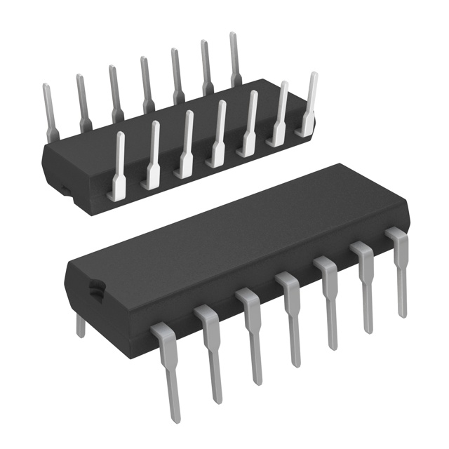
HEF4007UBP,652
IC DUAL PAIR/INVERTER 14-DIP
$0.12
View detail
NTS0304EUKZ
4-BIT VOLTAGE TRANSLATOR 12WLCSP
$0.66
View detail
SSTU32865ET/G,518
IC REG BUFFER 28BIT 160-TFBGA
$2.89
View detail
45
Serves customers in 45 countries
1000+
Worldwide Manufacturers
$140M
$140M Growth in 5 Years
50.0M+
50M Parts Shipped in 5 Years
Get in touch
Flat/Rm A 7/F Kimley Commercial Building 142-146 Queen's Road Central HK