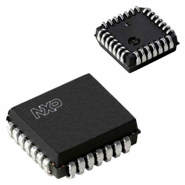
SSTV16857DGV,112
Compare
SSTV16857DGV,112
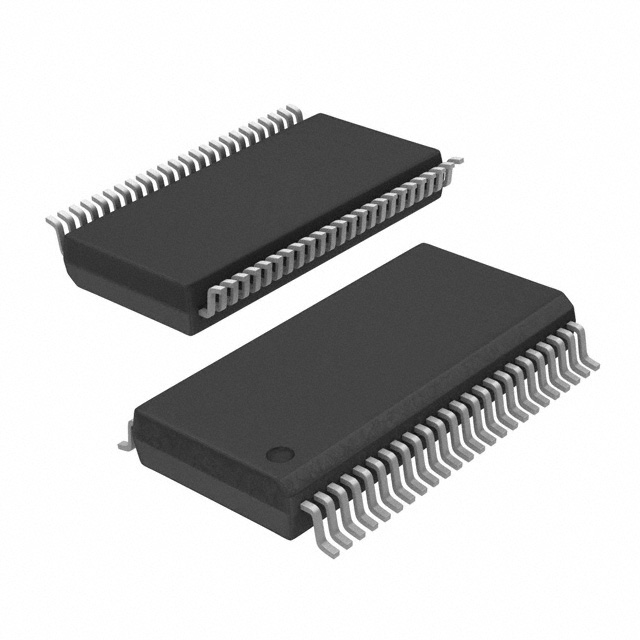
IC REG DRIVER 14BIT 48TSSOP
Compare
Obsolete
Quantity Available:
4860
SZC Quality Assurance


NXP USA Inc.
NXP Semiconductors, a frontrunner in embedded controllers, offers a wide array of MCUs with Arm-based processors. Their innovation extends to robust Power Management for industry and automotive use. NXP's products globally empower and interconnect, fostering proficiency for individuals, organizations, and the world. Noteworthy is the integration of Freescale Semiconductor into NXP (December 2015).
View All Product from NXP USA Inc.


SSTV16857DGV,112 FEATURES
• Stub-series terminated logic for 2.5 V VDDQ (SSTL_2)
• Optimized for DDR (Double Data Rate) SDRAM applications
• Inputs compatible with JESD8–9 SSTL_2 specifications.
• Flow-through architecture optimizes PCB layout
• ESD classification testing is done to JEDEC Standard JESD22.Protection exceeds 2000 V to HBM per method A114.
• Latch-up testing is done to JEDEC Standard JESD78, whichexceeds 100 mA.
• Same form, fit, and function as SSTL16877
• Full DDR 200/266 solution @ 2.5 V when used with PCKV857
• See SSTV16856 for driver/buffer version with mode select.
• Available in TSSOP-48, TVSOP-48 and 56 ball VFBGA packages
SSTV16857DGV,112 DESCRIPTION
The SSTV16857 is a 14-bit SSTL_2 registered driver with differentialclock inputs, designed to operate between 2.3 V and 2.7 V. VDDQmust not exceed VCC. Inputs are SSTL_2 type with VREF normally at0.5*VDDQ. The outputs support class I which can be used forstandard stub-series applications or capacitive loads. Master reset(RESET) asynchronously resets all registers to zero.The SSTV16857 is intended to be incorporated into standard DIMM(Dual In-Line Memory Module) designs defined by JEDEC, such asDDR (Double Data Rate) SDRAM or SDRAM II Memory Modules.Different from traditional SDRAM, DDR SDRAM transfers data onboth clock edges (rising and falling), thus doubling the peak busbandwidth. A DDR DRAM rated at 133 MHz will have a burst rate of266 MHz. The modules require between 23 and 27 registeredcontrol and address lines, so two 14-bit wide devices will be used oneach module. The SSTV16857 is intended to be used for SSTL_2input and output signals.The device data inputs consist of differential receivers. Onedifferential input is tied to the input pin while the other is tied to areference input pad, which is shared by all inputs.The clock input is fully differential to be compatible with DRAMdevices that are installed on the DIMM. However, since the controlinputs to the SDRAM change at only half the data rate, the devicemust only change state on the positive transition of the CLK signal.In order to be able to provide defined outputs from the device evenbefore a stable clock has been supplied, the device must support anasynchronous input pin (reset), which when held to the LOW statewill assume that all registers are reset to the LOW state and alloutputs drive a LOW signal as well.
SSTV16857DGV,112 PIN DESCRIPTION
• Optimized for DDR (Double Data Rate) SDRAM applications
Product Attributes
| TYPE | DESCRIPTION | Select all |
|---|---|---|
| Package | Tube | |
| Series | 74SSTV | |
| Supplier Device Package | 48-TSSOP | |
| Package / Case | 48-TFSOP (0.173", 4.40mm Width) | |
| Mounting Type | Surface Mount | |
| Operating Temperature | 0°C ~ 70°C | |
| Number of Bits | 14 | |
| Supply Voltage | 2.3V ~ 2.7V | |
| Logic Type | Registered Buffer with SSTL_2 Compatible I/O for DDR | |
| Product Status | Obsolete |
Obsolete
Quantity Available:
4860
SZC Quality Assurance
NXP USA Inc.
NXP Semiconductors, a frontrunner in embedded controllers, offers a wide array of MCUs with Arm-based processors. Their innovation extends to robust Power Management for industry and automotive use. NXP's products globally empower and interconnect, fostering proficiency for individuals, organizations, and the world. Noteworthy is the integration of Freescale Semiconductor into NXP (December 2015).
View All Product from NXP USA Inc.You May Also Be Interested In
More Electronic Parts More
74AUP1Z04GW/C125
BUS DRIVER, AUP/ULP/V SERIES
74HC283DB,112
IC 4BIT BINARY FULL ADDER 16SSOP
74ABT899A,623
IC 9BIT DUAL LATCH TXRX 28PLCC

NTS0304EPWJ
4-BIT VOLTAGE TRANSLATOR 14TSSOP
NTS0302JKZ
IC VOLT TRANSLATOR X2SON8

74AUP1Z125GF,132
BUS DRIVER, AUP/ULP/V SERIES, 1
74AUP1Z04GF132
NOW NEXPERIA 74AUP1Z04GF - BUS D
HEF4007UBP,652
IC DUAL PAIR/INVERTER 14-DIP
NTS0304EUKZ
4-BIT VOLTAGE TRANSLATOR 12WLCSP
SSTU32865ET/G,518
IC REG BUFFER 28BIT 160-TFBGA
45
Serves customers in 45 countries
1000+
Worldwide Manufacturers
$140M
$140M Growth in 5 Years
50.0M+
50M Parts Shipped in 5 Years