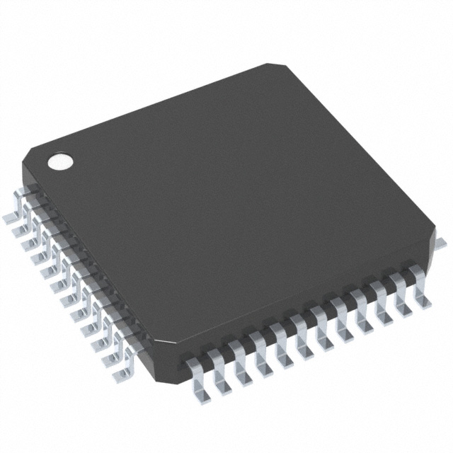
TLC320AD77CDB
Compare
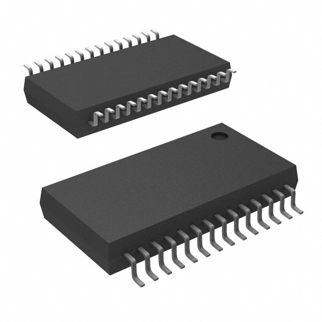
TLC320AD77CDB
IC CODEC AUDIO 24 BIT 28SSOP
Compare
$7.62
Quantity Available:
2500
SZC Quality Assurance


Texas Instruments
Texas Instruments Incorporated (TI) is a global semiconductor powerhouse, crafts advanced analog ICs and embedded processors. Fueled by top-tier minds, TI's innovations drive tech's future, impacting 100,000+ clients.
View All Product from Texas Instruments


TLC320AD77CDB Features
•24-Bit Delta Sigma Stereo ADC and DAC:–16-, 20-, or 24-Bit Input/Output Data–Wide Range of Sampling Rates: 16 kHz to 96 kHz–Master Clock: 256 fs or 384 fs–3.3-V Power Supply Operation–Internal Bandgap Voltage Reference–Economical 28-Pin DB (SSOP) Package
•Stereo ADC:–Differential Input–128× Oversampling (in normal speed mode)–High Performance: 100-dB Signal-to-Noise Ratio (SNR) (EIAJ), 100-dB Dynamic Range–Digital High-Pass Filter
•Stereo DAC:–Single-Ended Output–128× Oversampling (in normal speed mode)–High Performance: 100-dB Signal-to-Noise Ratio (SNR) (EIAJ), 100-dB Dynamic Range
•Digital De-Emphasis:–32-kHz, 44.1-kHz, and 48-kHz Selection
•Special Features:–High Jitter Tolerance–Good Phase Characteristics–Excellent Power Supply Rejection Ratio1–2
TLC320AD77CDB 2 Functional Description
2.1ADC ChannelTo produce excellent common-mode rejection of unwanted signals, the analog signal is processeddifferentially until it is converted to digital data. A single-ended input signal must be converted into adifferential input and filtered with a single-pole antialiasing filter before entering the ADC input. (SeeSection 2.7, ADC Analog Input). The ADC converts the signal into discrete output digital words in2s-complement format, corresponding to the analog signal input. There is a high-pass filter to get rid of anyoffset that the ADC modulator may have caused. These digital words, representing sampled values of theanalog input signal, are then clocked out the serial port, SDOUT, according to one of the eight allowableserial port protocols.2.2DAC ChannelSDIN receives a serial data word whose length is specified by one of the eight allowable serial port protocols,selected by the serial mode pins. The serial port latches the data on an edge of SCLK. The data goes throughthe sigma-delta DAC comprised of digital interpolation filters and a seventh order, 1-bit digital modulator.This oversampled signal is then passed through a switched capacitor FIR filter and RC low-pass filter whichsmoothes the output waveform, and performs the differential to single-ended conversion. The DAC outputsa stereo single-ended, inverted signal. This signal should be passed through an inverting,pseudo-differential, external low-pass filter, where the VCOM reference is subtracted out. (See Section 2.8,DAC Analog Output).2.3Serial InterfaceThe digital serial interface consists of a serial port, shift clock (SCLK), left/right frame synchronization clock(LRCLK), ADC-channel data output (SDOUT), and DAC-channel data input (SDIN). One of 8 different serialport modes may be selected including IIS, right/left justified, left/left justified, and a DSP mode for wordlengths ranging from 16 to 24 bits. See Section 2.14, Serial Interface Formats for a description of serialinterface formats.2.4Sampling FrequencyThe sampling or conversion frequency is designated by the MCLK rate by the following equation.fs = MCLK frequency/ (256 or 384).See Section 2.14, Serial Interface Formats for more information on the option of selecting an MCLK rateof 256 fs or 384 fs.2.5Speed Mode OptionsIn normal-speed mode (SPDMOD = 0), sampling frequencies ranging from 16 kHz up to 48 kHz should beused to achieve optimum performance.In high-speed mode (SPDMOD = 1) the sampling frequencies are greater than 48 kHz and up to 96 kHz.2.6Voltage ReferenceIn order to achieve excellent noise rejection, a pseudo-differential reference is used with external capacitorsconnected to a differential low-pass filter. The application schematic shows the necessary capacitorsneeded to complete the filters found on the device. See Section 5, Application Information for the applicationschematic for the voltage reference.2–22.7ADC Analog InputThe ADC accepts a differential input with a maximum value that does not exceed approximately 4 Vpp. SeeSection 5.1, Single-Ended to Differential External Analog Front-End Circuit for a description of therecommended external analog front end.2.8DAC Analog OutputThe DAC outputs a single-ended signal with a max value of 0.7 Vrms. See Section 5.2, External AnalogBack-End Circuit for a description of the recommended back-end circuit.2.9Sigma-Delta ADCThe sigma-delta ADC is a third order modulator with 128 times oversampling in normal speed operation.The ADC provides high resolution and low noise performance using over-sampling techniques.2.10 Decimation FilterThe decimation filter reduces the digital data rate to the sampling rate. This is accomplished by decimatingwith a ratio of 1:128. The output of this filter is a 2s complement 16-, 20-, 24-bit word clocking at the samplerate selected.2.11 Sigma-Delta DACThe sigma-delta DAC is a seventh order modulator with 128 times oversampling. The DAC provideshigh-resolution, low noise, from a 1-bit converter using over-sampling techniques.2.12 Interpolation FilterThe interpolation filter resamples the digital data at a rate 128 times the incoming sample rate. Thehigh-speed data output is then used in the sigma-delta DAC.2.13 De-emphasisDe-emphasis is supported for three sampling rates: 32 kHz, 44.1 kHz, and 48 kHz and selected with theDEM0 and DEM1 pins.2.14 Serial Interface FormatsThe TLC320AD77C operates only in slave mode. It requires externally supplied MCLK (master clock), andLRCLK (left/right clock), and SCLK (shift clock) inputs. There are two options for selecting the clock rates.If a 384 fs MCLK rate is selected, then a LRCLK frame of 48 SCLKs must be supplied. If a 256 fs MCLK isselected, then a LRCLK of 64 SCLKs must be supplied.
•A detection circuit automatically senses at which rate the MCLK is operating.
•The MCLK and SCLK must be synchronous and their edges must be at least 3 ns apart.
•If the LRCLK phase changes more than 10 MCLKs then the device automatically resets.The TLC320AD77C is compatible with eight different serial interfaces. Available interface options are IIS,right justified, left justified, and DSP frame. The following table indicates how the eight options are selectedusing the MOD0, MOD1, and MOD2 pins. All serial interface options at either 16-, 20-, or 24-bits can operatewith SCLK at 48*fs or 64*fs except for the 16-bit DSP mode which should use SCLK = 64 fs.2–3MODEMOD2 PINMOD1 PINMOD0 PINSERIAL INTERFACE SDIN (DAC)/SDOUT (ADC)000016-bit, MSB first, right justified/left justified100120-bit, MSB first, right justified/left justified201024-bit, MSB first, right justified/left justified301116-bit IIS410020-bit IIS510124-bit IIS611016-bit MSB first, left justified/left justified711116-bit DSP frame (see Note 1)NOTE 1:For the 16-bit DSP frame use SCLK = 64 fs.2.14.1MSB First Right/Left Justified FormatLeft ChannelRight ChannelMSBXLSBMSBXLSBMSBLSBSDOUTSDINLRCLK = fsSCLKMSBLSBFigure 2–1. MSB First Right/Left Justified (for 16-, 20-, and 24-bits)Note the following characteristics of this protocol.
•Left channel data is valid when LRCLK is high.
•The SDIN (recorded data) data is justified to the trailing edge of LRCLK
•The SDOUT MSB (playback data) is transmitted at the same time as the LRCLK edge, andcaptured at the very next rising edge of SCLK.
•If LRCLK phase changes by more than 10 MCLKs, then the device is automatically reset.2–42.14.2IIS-Compatible Serial FormatMSBXSDINSCLKMSBXLSBLSBMSBXMSBXLSBLSBLeft ChannelRight ChannelSDOUTLRCLK = fsFigure 2–2. IIS-Compatible Serial Format (for 16-, 20-, and 24-bits)Note the following characteristics of this protocol.
•Left channel data is valid when LRCLK is low.
•SDIN is sampled with the rising edge of SCLK.
•SDOUT is transmitted on the falling edge of SCLK.
•If LRCLK phase changes by more than 10 MCLKs, then the device is automatically reset.2.14.3MSB Left Justified Serial Interface FormatMSBMSBMSBMSBLSBLSBLeft ChannelRight ChannelSDINSCLKSDOUTLRCLK = fsLSBLSBFigure 2–3. MSB Left Justified Serial Interface Format (for 16-bits)Note the following characteristics of this protocol.
•Left channel data is valid when LRCLK is high.
•The SDIN data is justified to the leading edge of LRCLK.
•The MSBs are valid at the same time as the LRCLK edge for SDOUT, and captured at the verynext rising edge of SCLK for SDIN.2–52.14.4DSP Compatible Serial Interface Format1514131514130015141315141300Left Channel(MSB = 15)Right Channel(MSB = 15)SDINSCLKSDOUTLRCLK = fsFigure 2–4. DSP Compatible Serial Interface Format (for 16-bits)Note the following characteristics of this protocol.
•MCLK = 256 Fs only
•SCLK = 64 times the sampling frequency.
•Serial data is sampled with the falling edge of SCLK.
•Serial data is transmitted on the rising edge of SCLK.2.15 Sampling Frequency RangesThe TLC320AD77C supports two sampling frequency ranges.
•When in the normal option ranging from 16 kHz up to 48 kHz, SPDMOD = low is used.
•When in the fast option ranging from greater than 48 kHz up to 96 kHz, SPDMOD = high is used.NOTE:The high speed clocks should never be applied while SPDMOD is low in order toavoid glitches in the DAC and ADC outputs.Table 2–1. Example Master Clock Frequency RatesSAMPLING RATE FREQUENCYMCLK FREQUENCYSPDMODE(kHz)256 fs384 fsSPDMODE328.192 MHz12.2880 MHz044.111.2896 MHz16.9340 MHz04812.2880 MHz18.432 MHz06416.384 MHz24.576 MHz188.222.579 MHz33.868 MHz19624.576 MHz36.864 MHz12.16 Power Sequences2.16.1Initial Power UpFor initial power up, the ADC and DAC outputs are valid after the 150 ms settling time required for the analogstages. Holding the power down pin low while ramping up the power supplies is recommended to avoidglitches in the DAC output.2–62.16.2Power Down/ResetThe TLC320AD77C is capable of entering a stand-by mode at reduced power when no activity is required.To initiate the reset sequence, PDN_RSTB is held low for a minimum of 10 ns. As long as the pin is heldlow, the device is in the power-down state.In order for the dynamic logic to be properly powered down, the clocks should not be stopped before thePDN_RSTB pin goes low. Otherwise, the device may drain additional supply current.2.16.3Reinitialization SequenceWhen PDN_RSTB is returned to high, the device begins a reinitialization sequence after all clocks areactive. The output data becomes valid after a minimum of 128 LRCLK cycles after the pin is pulled high.During the initialization sequence the outputs of the DAC and ADC are invalid.Any change in the control lines (MOD0, MOD1, MOD2, DEM0, DEM1, SPDMOD, PDN_RST) or phase shiftin LRCLK triggers the reinitialization sequence.In order for the dynamic logic to be properly powered down, the clocks should not be stopped before thePDN_RSTB pin goes low. Otherwise, the device may drain additional supply current.2.17 DAC De-Emphasis FilterDe-emphasis is only supported for three sampling rates (fs): 32 kHz, 44.1 kHz, and 48 kHz in normal speedoperation. The DEM0 and DEM1 pins select the filter coefficients and enable or disable the filter. Figure 2–5illustrates the de-emphasis filtering characteristics.0–103.18(50 µs)10.6(15 µs)f – Frequency – kHzResponse – dBDe-emphasisFigure 2–5. De-Emphasis Characteristics2.17.1De-Emphasis SelectionDe-emphasis control is achieved using the DEM1 and DEM0 pins. The pin control is defined in the followingtable.DEM 1DEM 0DE-EMPHASIS0032 kHz0144.1 kHz1048 kHz11Off3–1
Product Attributes
| TYPE | DESCRIPTION | Select all |
|---|---|---|
| S/N Ratio, ADCs / DACs (db) Typ | 100 / 100 | |
| Sigma Delta | Yes | |
| Number of ADCs / DACs | 1 / 1 | |
| Resolution (Bits) | 24 b | |
| Data Interface | Serial | |
| Supplier Device Package | 28-SSOP | |
| Package / Case | 28-SSOP (0.209", 5.30mm Width) | |
| Type | Stereo Audio | |
| Product Status | Obsolete | |
| Mounting Type | Surface Mount | |
| Package | Tube | |
| Operating Temperature | 0°C ~ 70°C | |
| Series | - | |
| Voltage - Supply, Digital | 3V ~ 3.6V | |
| Voltage - Supply, Analog | 3V ~ 3.6V | |
| Dynamic Range, ADCs / DACs (db) Typ | 100 / 100 |
$7.62
Quantity Available:
2500
SZC Quality Assurance
Texas Instruments
Texas Instruments Incorporated (TI) is a global semiconductor powerhouse, crafts advanced analog ICs and embedded processors. Fueled by top-tier minds, TI's innovations drive tech's future, impacting 100,000+ clients.
View All Product from Texas InstrumentsYou May Also Be Interested In
More Electronic Parts More
TP3067V-X
MONOLITHIC SERIAL INTERFACE CMOS
TP3054N
PCM CODEC MU-LAW 1-FUNC PDIP16
TP3071N-G
PROGRAMMABLE CODEC, A/MU-LAW, 1-
TLV320AIC3104IRHBR
IC AUDIO CODEC 24BIT SER 32VQFN
PCM3168APAPR
IC CODEC AUDIO 24 BIT 64HTQFP
PCM2900CDBR
IC STEREO AUD CODEC W/USB 28SSOP
TLV320AIC3254IRHBT
IC STEREO AUDIO CODEC 1.8V 32QFN
LM4550BVH/NOPB
IC AC '97 AUDIO CODEC 48-LQFP
TLV320AIC34IZAS
IC AUDIO CODEC 24BIT PCM 87BGA
PCM2906CDB
IC STEREO AUD CODEC W/USB 28SSOP
45
Serves customers in 45 countries
1000+
Worldwide Manufacturers
$140M
$140M Growth in 5 Years
50.0M+
50M Parts Shipped in 5 Years