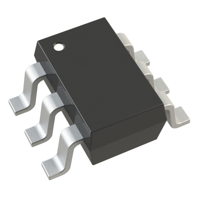
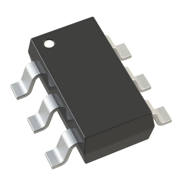
AD8312ACBZ-P7
Compare
AD8312ACBZ-P7
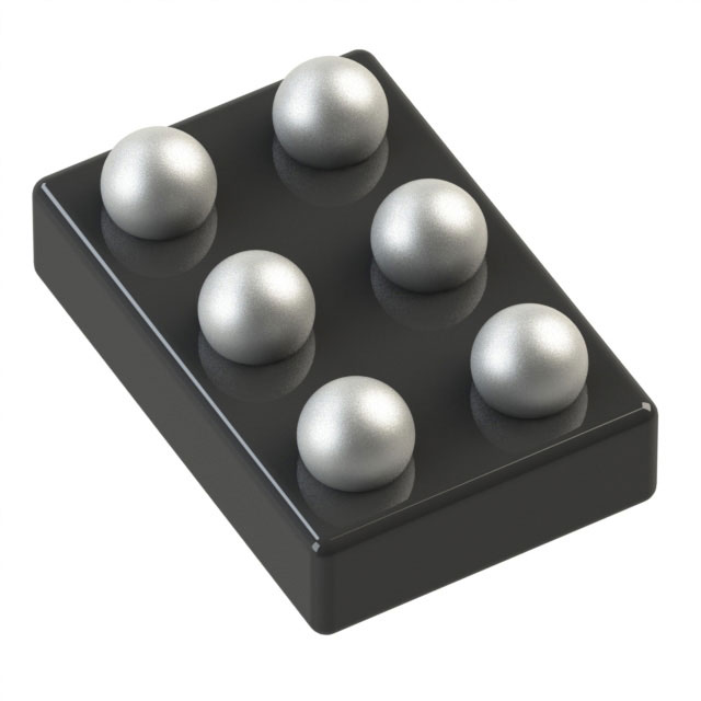
IC RF DETECT 50MHZ-3.5GHZ 6CSP
Compare
$1.00
Quantity Available:
12800
SZC Quality Assurance


Analog Devices Inc.
Analog Devices (NASDAQ: ADI) leads in crafting high-performance analog, mixed-signal, and digital signal processing integrated circuits. For decades, they've tackled signal processing challenges across global electronics. With over 100,000 clients, their products convert real-world phenomena into electrical signals. Merged with Maxim Integrated, they offer top-tier mixed-signal and power management technologies, solving complex problems from DC to 100 GHz and sensor to cloud.
View All Product from Analog Devices Inc.


AD8312ACBZ-P7 FEATURES
Complete RF detector functionTypical range: −45 dBm to 0 dBm, referencing 50 ΩFrequency response from 50 MHz to 3.5 GHzTemperature stable linear in dB responseAccurate to 3.5 GHzRapid response: 85/120 ns (rise/fall)Low power: 12 mW at 2.7 V
AD8312ACBZ-P7 GENERAL DESCRIPTION
The AD8312 is a complete, low cost subsystem for themeasurement of radio frequency (RF) signals in the frequencyrange of 50 MHz to 3.5 GHz. It has a typical dynamic range of45 dB and is intended for use in a wide variety of cellular handsetsand other wireless devices. It provides a wider dynamic rangeand better accuracy than possible using discrete diode detectors. Inparticular, its temperature stability is excellent over the fulloperating range of −40°C to +85°C. Its high sensitivity allowsmeasurement at low power levels, thus reducing the amount ofpower that needs to be coupled to the detector. It is essentially avoltage responding device, with a typical signal range of 1.25 mVto 224 mV rms or −45 dBm to 0 dBm, referencing 50 Ω.For convenience, the signal is internally ac-coupled, using a5 pF capacitor to a load of 3 kΩ in shunt with 1.3 pF. This high-pass coupling, with a corner at approximately 16 MHz, determinesthe lowest operating frequency. Therefore, the source may be dcgrounded.The AD8312 output, VOUT, increases from close to ground toabout 1.2 V because the input signal level increases from 1.25 mVto 224 mV. A capacitor may be connected between the VOUTand CFLT pins when it is desirable to increase the time intervalover which averaging of the input waveform occurs.The AD8312 is available in a 6-ball, 1.0 mm × 1.5 mm, waferlevel chip scale package and consumes 4.2 mA from a 2.7 V to5.5 V supply.
AD8312ACBZ-P7 APPLICATIONS
Cellular handsets (GSM, CDMA, WCDMA)RSSI and TSSI for wireless terminal devicesTransmitter power measurement
Product Attributes
| TYPE | DESCRIPTION | Select all |
|---|---|---|
| Mounting Type | Surface Mount | |
| Current - Supply | 5.7 mA | |
| Voltage - Supply | 2.7V ~ 5.5V | |
| Accuracy | ±1dB | |
| Input Range | -45dBm ~ 0dBm | |
| RF Type | Cellular, GSM, CDMA, W-CDMA | |
| Frequency | 50MHz ~ 3.5GHz | |
| Product Status | Active | |
| Package | Strip | |
| Series | - | |
| Supplier Device Package | 6-WLCSP (1.45x0.95) | |
| Package / Case | 6-WFBGA, WLCSP |
$1.00
Quantity Available:
12800
SZC Quality Assurance
Analog Devices Inc.
Analog Devices (NASDAQ: ADI) leads in crafting high-performance analog, mixed-signal, and digital signal processing integrated circuits. For decades, they've tackled signal processing challenges across global electronics. With over 100,000 clients, their products convert real-world phenomena into electrical signals. Merged with Maxim Integrated, they offer top-tier mixed-signal and power management technologies, solving complex problems from DC to 100 GHz and sensor to cloud.
View All Product from Analog Devices Inc.You May Also Be Interested In
More Electronic Parts MoreAD8312ACBZ-P7
IC RF DETECT 50MHZ-3.5GHZ 6CSP
AD8314ACPZ-RL7
IC RF DETECT 100MHZ-2.7GHZ 8CSP
LTC5505-2ES5#TRMPBF
IC RF DETECT 300MZ-3.5GHZ TSOT23
LT5581IDDB#TRMPBF
IC RF DETECT 10MHZ-6GHZ 8DFN
ADL5501AKSZ-R7
IC RF DETECT 50MHZ-6GHZ SC70-6
AD8361ARTZ-RL7
IC RF DETECT 100MHZ-2.5GHZ SOT23
AD8318ACPZ-REEL7
IC RF DETECT 1MHZ-8GHZ 16LFCSP
LT5538IDD#PBF
IC RF DETECT 40MHZ-3.8GHZ 8DFN
HMC1120LP4ETR
IC RF DETECT 0HZ-3.9GHZ 24QFN
LTC5582IDD#PBF
IC RF DETECT 40MHZ-10GHZ 10DFN
45
Serves customers in 45 countries
1000+
Worldwide Manufacturers
$140M
$140M Growth in 5 Years
50.0M+
50M Parts Shipped in 5 Years