All categories
- All categories
- Integrated Circuits (ICs)
- Development Boards, Kits, Programmers
- Discrete Semiconductor Products
- Power Supplies - Board Mount
- RF and Wireless
- Sensors, Transducers
- Memory Cards, Modules
- Audio Products
- Circuit Protection
- Crystals, Oscillators, Resonators
- Filters
- Isolators
- Kits
- Maker/DIY, Educational
- Optoelectronics
- Power Supplies - External/Internal (Off-Board)
- Relays
- Resistors
- Test and Measurement
- Uncategorized
- Inductors, Coils, Chokes
- Motors, Actuators, Solenoids and Drivers
- Switches
- Embedded Computers
- Capacitors
- Transformers
- Battery Products
- Products
- All categories
-
Integrated Circuits (ICs)
-
Embedded
- FPGAs (Field Programmable Gate Array)
- Microcontrollers
- CPLDs (Complex Programmable Logic Devices)
- FPGAs (Field Programmable Gate Array) with Microcontrollers
- PLDs (Programmable Logic Device)
- Microcontrollers, Microprocessor, FPGA Modules
- System On Chip (SoC)
- Application Specific Microcontrollers
- DSP (Digital Signal Processors)
- Microprocessors
-
Interface
- Drivers, Receivers, Transceivers
- Sensor and Detector Interfaces
- Analog Switches - Special Purpose
- Analog Switches, Multiplexers, Demultiplexers
- CODECS
- Controllers Interface ICs
- Direct Digital Synthesis (DDS)
- Encoders, Decoders, Converters
- Filters - Active
- I/O Expanders
- Modems - ICs and Modules
- Modules
- Sensor, Capacitive Touch
- Signal Buffers, Repeaters, Splitters
- Signal Terminators
- Specialized
- Telecom
- Serializers, Deserializers
- UARTs (Universal Asynchronous Receiver Transmitter)
- Voice Record and Playback
- Memory
-
Power Management (PMIC)
- DC DC Switching Controllers
- Display Drivers
- Full Half-Bridge Drivers
- Gate Drivers
- LED Drivers
- Motor Drivers, Controllers
- Power Distribution Switches, Load Drivers
- Power Management - Specialized
- Power Supply Controllers, Monitors
- Special Purpose Regulators
- Supervisors
- Voltage Regulators - DC DC Switching Regulators
- Voltage Regulators - Linear
- Voltage Regulators - Linear + Switching
- AC DC Converters, Offline Switches
- Battery Chargers
- Battery Management
- Current Regulation/Management
- Energy Metering
- Hot Swap Controllers
- Laser Drivers
- Lighting, Ballast Controllers
- OR Controllers, Ideal Diodes
- PFC (Power Factor Correction)
- Power Over Ethernet (PoE) Controllers
- RMS to DC Converters
- Thermal Management
- Voltage Reference
- Voltage Regulators - Linear Regulator Controllers
- V/F and F/V Converters
- Specialized ICs
- Audio Special Purpose
- Clock/Timing
- Data Acquisition
- Linear
-
Logic
- Buffers, Drivers, Receivers, Transceivers
- Comparators
- FIFOs Memory
- Flip Flops
- Gates and Inverters
- Gates and Inverters - Multi-Function, Configurable
- Multivibrators
- Shift Registers
- Signal Switches, Multiplexers, Decoders
- Translators, Level Shifters
- Latches
- Specialty Logic
- Counters, Dividers
- Parity Generators and Checkers
- Universal Bus Functions
-
Embedded
-
Development Boards, Kits, Programmers
- Accessories
- Evaluation and Demonstration Boards and Kits
- Evaluation Boards - DC/DC & AC/DC (Off-Line) SMPS
- Evaluation Boards - Expansion Boards, Daughter Cards
- Evaluation Boards - LED Drivers
- Evaluation Boards - Sensors
- Evaluation Boards - Embedded - Complex Logic (FPGA, CPLD)
- Evaluation Boards - Embedded - MCU, DSP
- Programmers, Emulators, and Debuggers
- Software, Services
- Evaluation Boards - Analog to Digital Converters (ADCs)
- Evaluation Boards - Audio Amplifiers
- Evaluation Boards - Digital to Analog Converters (DACs)
- Evaluation Boards - Linear Voltage Regulators
- Evaluation Boards - Op Amps
- Programming Adapters, Sockets
- RF Evaluation and Development Kits, Boards
- RFID Evaluation and Development Kits, Boards
-
Discrete Semiconductor Products
- Power Supplies - Board Mount
-
RF and Wireless
- RF Amplifiers
- Attenuators
- RF Accessories
- RF Demodulators
- RF Detectors
- RF Front End (LNA + PA)
- RF Misc ICs and Modules
- RF Mixers
- RF Modulators
- RF Power Controller ICs
- RF Power Dividers/Splitters
- RF Receivers
- RF Shields
- RF Switches
- RF Transceiver ICs
- RF Transceiver Modules and Modems
- RF Transmitters
- RFID, RF Access, Monitoring ICs
- RFID Transponders, Tags
- RF Multiplexers
- RF Receiver, Transmitter, and Transceiver Finished Units
- RF Antennas
- RFI and EMI - Contacts, Fingerstock and Gaskets
- RFID Reader Modules
- RF Circulators and Isolators
- RF Directional Coupler
- Balun
- Subscriber Identification Module (SIM) Cards
- RFID Accessories
- RFID Antennas
-
Sensors, Transducers
- Current Sensors
- Magnetic Sensors
- Position Sensors
- Specialized Sensors
- Temperature Sensors
- Motion Sensors
- Multifunction
-
Optical Sensors
- Ambient Light, IR, UV Sensors
- Image Sensors, Camera
- Photodiodes
- Distance Measuring
- Photointerrupters - Slot Type - Transistor Output
- Phototransistors
- Reflective - Analog Output
- Reflective - Logic Output
- Photo Detectors - Logic Output
- Photointerrupters - Slot Type - Logic Output
- Photoelectric, Industrial
- Camera Modules
- Photo Detectors - Remote Receiver
- Sensor, Transducer Accessories
- Sensor, Transducer Amplifiers
- Color Sensors
- Encoders
- Encoders - Industrial
- Touch Sensors
- Pressure Sensors, Transducers
- Flow Sensors
- Gas Sensors
- Pressure Sensors, Transducers - Industrial
- Float, Level Sensors
- Magnets
- Proximity Sensors
- Flow Sensors - Industrial
- Humidity, Moisture Sensors
- Memory Cards, Modules
- Audio Products
- Circuit Protection
- Crystals, Oscillators, Resonators
- Filters
- Isolators
- Kits
- Maker/DIY, Educational
-
Optoelectronics
- Circuit Board Indicators, Arrays, Light Bars, Bar Graphs
- Fiber Optic Transceiver Modules
- LED Character and Numeric
- COBs, Engines, Modules, Strips
- Color LED Lighting
- Display Bezels, Lenses
- Fiber Optic Receivers
- Fiber Optic Transmitters - Discrete
- Fiber Optic Transmitters - Drive Circuitry Integrated
- Laser Diodes, Modules
- LED Dot Matrix and Cluster
- LED Emitters - Infrared, UV, Visible
- LED Indication - Discrete
- Lenses
- Optoelectronics Accessories
- White LED Lighting
- Incandescent, Neon Lamps
- Fiber Optic Switches, Multiplexers, Demultiplexers
- Ballasts, Inverters
- LCD, OLED, Graphic
- LCD, OLED Character and Numeric
- Display, Monitor - LCD Driver/Controller
- Power Supplies - External/Internal (Off-Board)
- Relays
- Resistors
- Test and Measurement
- Uncategorized
- Inductors, Coils, Chokes
- Motors, Actuators, Solenoids and Drivers
- Switches
- Embedded Computers
- Capacitors
- Transformers
- Battery Products
- Manufacturers
- Services
- Industries
- Top-Quality Commitment
- Resources

ADRF5515BCPZN-R7 datasheet
ADRF5515BCPZN-R7 pdf
ADRF5515BCPZN-R7 distributor
ADRF5515BCPZN-R7 manufacturer
ADRF5515BCPZN-R7 supplier
ADRF5515BCPZN-R7 price
ADRF5515BCPZN-R7 specification
ADRF5515BCPZN-R7 wholesale
ADRF5515BCPZN-R7 package
ADRF5515BCPZN-R7 Analog Devices Inc.
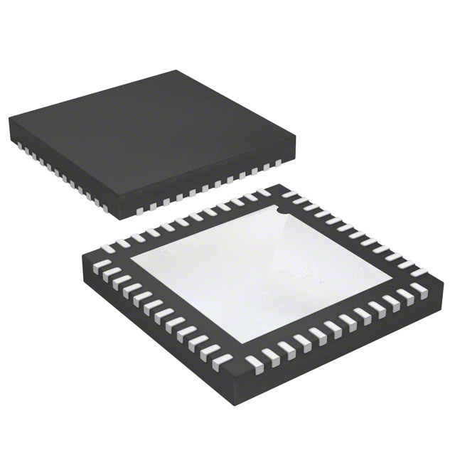
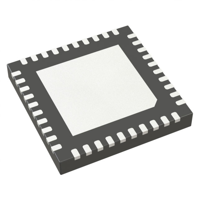
ADRF5515BCPZN-R7
Compare
ADRF5515BCPZN-R7
3.6 GHZ RECEIVER FRONT END
Compare
$14.64
Quantity Available:
3718
SZC Quality Assurance


Analog Devices Inc.
Analog Devices (NASDAQ: ADI) leads in crafting high-performance analog, mixed-signal, and digital signal processing integrated circuits. For decades, they've tackled signal processing challenges across global electronics. With over 100,000 clients, their products convert real-world phenomena into electrical signals. Merged with Maxim Integrated, they offer top-tier mixed-signal and power management technologies, solving complex problems from DC to 100 GHz and sensor to cloud.
View All Product from Analog Devices Inc.


Product Details
Shipping
Quality Guarantee
Reviews
ADRF5515BCPZN-R7 FEATURES
Integrated dual-channel RF front end2-stage LNA and high power silicon SPDT switchOn-chip bias and matchingSingle-supply operationGainHigh gain mode: 33 dB typical at 3.6 GHzLow gain mode: 16 dB typical at 3.6 GHzLow noise figureHigh gain mode: 1.0 dB typical at 3.6 GHzLow gain mode: 1.0 dB typical at 3.6 GHzHigh isolationRXOUT-CHA and RXOUT-CHB: 45 dB typicalTERM-CHA and TERM-CHB: 60 dB typicalLow insertion loss: 0.45 dB typical at 3.6 GHzHigh power handling at TCASE = 105°CFull lifetimeLTE average power (9 dB PAR): 43 dBmHigh OIP3 (high gain mode): 32 dBm typicalPower-down mode and low gain mode for LNALow supply currentHigh gain mode: 86 mA typical at 5 VLow gain mode: 36 mA typical at 5 VPower-down mode: 12 mA typical at 5 VPositive logic control6 mm × 6 mm, 40-lead LFCSPPin compatible with the ADRF5545A, 10 W version
ADRF5515BCPZN-R7 GENERAL DESCRIPTION
The ADRF5515 is a dual-channel, integrated RF, front-end,multichip module designed for time division duplexing (TDD)applications. The device operates from 3.3 GHz to 4.0 GHz.The ADRF5515 is configured in dual channels with a cascading,two-stage, LNA and a high power silicon SPDT switch.In high gain mode, the cascaded two-stage LNA and switchoffer a low noise figure of 1.0 dB and a high gain of 33 dB at3.6 GHz with an output third-order intercept point (OIP3) of32 dBm (typical). In low gain mode, one stage of the two-stageLNA is in bypass, providing 16 dB of gain at a lower current of36 mA. In power-down mode, the LNAs are turned off and thedevice draws 12 mA.
ADRF5515BCPZN-R7 APPLICATIONS
Wireless infrastructureTDD massive multiple input and multiple output and activeantenna systemsTDD-based communication systems
Shipping Cost
- 1. Shipping starts at $40, but prices may vary for certain countries like South Africa, Brazil, India, Pakistan, Israel, etc.
- 2. The basic freight for packages ≤0.5kg or equivalent volume is influenced by the time zone and country.
Shipping Method
- 1. Our products are currently shipped using DHL, SF, and UPS. For low quantities, FedEx is the chosen carrier.
Delivery Time
- 1. Once shipped, the estimated delivery time is contingent on the selected shipping method.
1. Every electronic component you purchase from us comes with a 365-Day Warranty. We stand behind the quality of our products.
2. Should you receive any item that isn't in perfect condition, we are committed to arranging a refund or replacement responsibly. Please note that items must be in their original condition for these options to be available.
FAQs:Q: How does SZComponents ensure that ADRF5515BCPZN-R7 is genuinely manufactured or distributed by ?
A: Our professional business development department conducts rigorous testing and verification of the qualifications of original manufacturers and agents of . All suppliers must undergo and pass our qualification review before they are allowed to list their ADRF5515BCPZN-R7 devices on our platform. We prioritize the sourcing channels and quality of ADRF5515BCPZN-R7 products above everything else, ensuring thorough supplier audits so you can make your purchase with utmost confidence.
Q: Where can I find detailed information about ADRF5515BCPZN-R7 chips, including original manufacturer details, RF Front End (LNA + PA) application, and images?
A: Utilize SZComponents's intelligent search engine, filter by the RF Front End (LNA + PA) category, or navigate through the 's brand page for comprehensive information.
Q: Are the prices and stock levels of 's ADRF5515BCPZN-R7 shown on the platform accurate?
A: Due to significant fluctuations in 's inventory, real-time updates are challenging. However, we ensure periodic updates within 24 hours. We recommend confirming your ADRF5515BCPZN-R7 order with a SZComponents sales representative or through our online customer service before proceeding with payment.
Q: What payment methods are accepted by SZComponents?
A: We accept various payment methods, including TT Bank, PayPal, Credit Card, Western Union, and Escrow.
Q: How are shipping arrangements made, and how can I track my package?
A: Customers can select from industry-leading freight companies like DHL, FedEx, UPS, TNT, and Registered Mail. Once your order is ready for shipment, our sales team will inform you about the shipping details and provide a tracking number. Note that tracking information might take up to 24 hours to appear. Typically, Express delivery takes 3-5 days, while Registered Mail requires 25-60 days.
Q: What is the process for returns or replacements of ADRF5515BCPZN-R7?
A: We conduct a Pre-Shipment Inspection (PSI) on randomly selected batches from your order to ensure quality before shipment. We will accept returns or replacements of the ADRF5515BCPZN-R7 if it does not meet your expectations under the following conditions:
- Issues such as incorrect quantities, delivery of wrong items, or obvious external defects are acknowledged by us.
- We are informed about the defects within 90 days from the delivery date.
- The ADRF5515BCPZN-R7 remains unused and in its original packaging.
- To initiate a return, please:
- Inform us within the 90-day period.
- Obtain a Request for Return Authorization.
- For more details, refer to our Return & Change Policy.
Q: How can I get support or request datasheets and pin diagrams for ADRF5515BCPZN-R7?
A: For any After-Sales service, including datasheets and pin diagrams for ADRF5515BCPZN-R7, feel free to contact us at [email protected]
Q: How can I contact SZComponents? Please provide specific contact methods.
A: Reach out to us by clicking the customer service button at the bottom right corner of our site, submitting an RFQ directly, or using the 'Contact Us' link at the top of our page to email or call us. We guarantee a response to your inquiries within 24 hours.
Q: How does SZComponents ensure that ADRF5515BCPZN-R7 is genuinely manufactured or distributed by ?
A: Our professional business development department conducts rigorous testing and verification of the qualifications of original manufacturers and agents of . All suppliers must undergo and pass our qualification review before they are allowed to list their ADRF5515BCPZN-R7 devices on our platform. We prioritize the sourcing channels and quality of ADRF5515BCPZN-R7 products above everything else, ensuring thorough supplier audits so you can make your purchase with utmost confidence.
Q: Where can I find detailed information about ADRF5515BCPZN-R7 chips, including original manufacturer details, RF Front End (LNA + PA) application, and images?
A: Utilize SZComponents's intelligent search engine, filter by the RF Front End (LNA + PA) category, or navigate through the 's brand page for comprehensive information.
Q: Are the prices and stock levels of 's ADRF5515BCPZN-R7 shown on the platform accurate?
A: Due to significant fluctuations in 's inventory, real-time updates are challenging. However, we ensure periodic updates within 24 hours. We recommend confirming your ADRF5515BCPZN-R7 order with a SZComponents sales representative or through our online customer service before proceeding with payment.
Q: What payment methods are accepted by SZComponents?
A: We accept various payment methods, including TT Bank, PayPal, Credit Card, Western Union, and Escrow.
Q: How are shipping arrangements made, and how can I track my package?
A: Customers can select from industry-leading freight companies like DHL, FedEx, UPS, TNT, and Registered Mail. Once your order is ready for shipment, our sales team will inform you about the shipping details and provide a tracking number. Note that tracking information might take up to 24 hours to appear. Typically, Express delivery takes 3-5 days, while Registered Mail requires 25-60 days.
Q: What is the process for returns or replacements of ADRF5515BCPZN-R7?
A: We conduct a Pre-Shipment Inspection (PSI) on randomly selected batches from your order to ensure quality before shipment. We will accept returns or replacements of the ADRF5515BCPZN-R7 if it does not meet your expectations under the following conditions:
- Issues such as incorrect quantities, delivery of wrong items, or obvious external defects are acknowledged by us.
- We are informed about the defects within 90 days from the delivery date.
- The ADRF5515BCPZN-R7 remains unused and in its original packaging.
- To initiate a return, please:
- Inform us within the 90-day period.
- Obtain a Request for Return Authorization.
- For more details, refer to our Return & Change Policy.
Q: How can I get support or request datasheets and pin diagrams for ADRF5515BCPZN-R7?
A: For any After-Sales service, including datasheets and pin diagrams for ADRF5515BCPZN-R7, feel free to contact us at [email protected]
Q: How can I contact SZComponents? Please provide specific contact methods.
A: Reach out to us by clicking the customer service button at the bottom right corner of our site, submitting an RFQ directly, or using the 'Contact Us' link at the top of our page to email or call us. We guarantee a response to your inquiries within 24 hours.
5.0
Product Attributes
| TYPE | DESCRIPTION | Select all |
|---|---|---|
| Supplier Device Package | 40-LFCSP-VQ (6x6) | |
| Package / Case | 40-VFQFN Exposed Pad, CSP | |
| Features | - | |
| Frequency | 3.3GHz ~ 4GHz | |
| RF Type | General Purpose | |
| Product Status | Active | |
| Package | Tape & Reel (TR) | |
| Series | - |
Similar parts:0
$14.64
Quantity Available:
3718
SZC Quality Assurance
Analog Devices Inc.
Analog Devices (NASDAQ: ADI) leads in crafting high-performance analog, mixed-signal, and digital signal processing integrated circuits. For decades, they've tackled signal processing challenges across global electronics. With over 100,000 clients, their products convert real-world phenomena into electrical signals. Merged with Maxim Integrated, they offer top-tier mixed-signal and power management technologies, solving complex problems from DC to 100 GHz and sensor to cloud.
View All Product from Analog Devices Inc.You May Also Be Interested In
More Electronic Parts MoreADRF5515BCPZN-R7
3.6 GHZ RECEIVER FRONT END
$14.64
View detail
AD9864BCPZRL
IC IF SUBSYSTEM GEN-PURP 48LFCSP
$27.16
View detail

ADRF5545ABCPZN-R7
DUAL CHANNEL, 2.4 GHZ TO 4.2 GHZ
$25.92
View detail

ADRF5515BCPZN
3.6 GHZ RECEIVER FRONT END
$20.50
View detail

ADRF5545ABCPZN
DUAL CHANNEL, 2.4 GHZ TO 4.2 GHZ
$25.92
View detail
ADRF5547BCPZN
4.0 - 5.5GHZ LNA + 40W SPDT, DUA
$25.92
View detail

ADRF5549BCPZN
1.8 - 2.8GHZ LNA + 40W SPDT, DUA
$25.92
View detail
AD9863BCPZ-50
IC FRONT-END MIXED-SGNL 64-LFCSP
$57.13
View detail
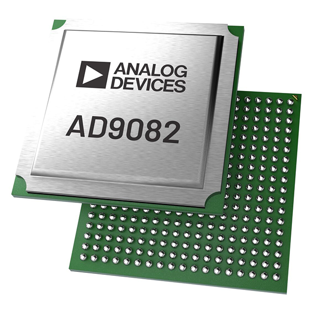
AD9082BBPZ-4D2AC
QUAD 12 GSPS RFDAC DUAL 6GSPS RF
$2,206.88
View detail

ADRF5519BCPZN
2.6 GHZ RECEIVER FRONT END
$21.73
View detail
45
Serves customers in 45 countries
1000+
Worldwide Manufacturers
$140M
$140M Growth in 5 Years
50.0M+
50M Parts Shipped in 5 Years
Get in touch
Flat/Rm A 7/F Kimley Commercial Building 142-146 Queen's Road Central HK