$57.82
Quantity Available:
4143
SZC Quality Assurance


Texas Instruments
Texas Instruments Incorporated (TI) is a global semiconductor powerhouse, crafts advanced analog ICs and embedded processors. Fueled by top-tier minds, TI's innovations drive tech's future, impacting 100,000+ clients.
View All Product from Texas Instruments


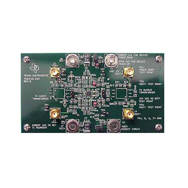
THS4130EVM Evaluation Module Features
THS4130 high-speed operational amplifier EVM features include:�Voltage supply operation range: 5-V to ±15-V operation (see thedevice data sheet)�Single and differential input and output capability�Nominal 50-Ω input and output termination resistors. They can beconfigured according to the application requirement.�VOCM direct input control (see schematic and the device data sheet)�VOCM pin can be controlled via transformer center-tap (seeschematic)�Shutdown pin control, JU1 (if applicable to the device, see the devicedata sheet)�Input and output transformer footprints for changing single-endedsignals to differential signals�Footprint for high-precision, balanced feedback and gain resistors(0.01% or better)�Footprints for low-pass filter implementation (see application noteSLOA054A)�Footprints for antialiasing filter implementation (see application noteSLOA054A)�Differential probe terminals on input and output nodes for differentialprobe insertion�Various GND and signal test points on the PCB�Circuit schematic printed on the back of the EVM�A good example of high-speed amplifier PCB design and layoutTHS4130 EVM Specifications1-3Introduction and Description
THS4130EVM Introduction and Description
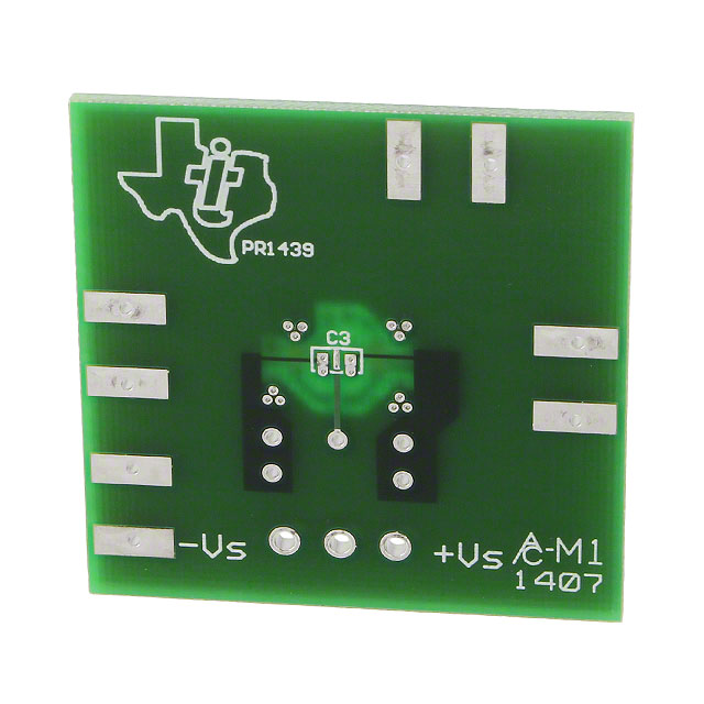
The Texas Instruments THS4130 evaluation module (EVM) helps designersevaluate the performance of the THS4130 operational amplifier. Also, thisEVM is a good example of high-speed PCB design.This document details the Texas Instruments THS4130 high-speedoperational amplifier evaluation module (EVM). It includes a list of EVMfeatures, a brief description of the module illustrated with a series of schematicdiagrams, EVM specifications, details on connecting and using the EVM, anda discussion of high-speed amplifier design considerations.This EVM enables the user to implement various circuits to clarify the availableconfigurations presented by the schematic of the EVM. In addition, theschematic of the default circuit has been added to depict the componentsmounted on the EVM when it is received by the customer. This configurationcorrelates to the single input/differential output signal.Other sample circuits are presented to show how the user can implement othercircuit configurations such as differential input/differential output signal,transformer utilization on the input and output terminals, VICR level shifter,and Butterworth filter with multiple feedback. The user may be able to createand implement circuit configurations in addition to those presented in thisdocument using the THS4130 EVM.TopicPage1.1Description1-2. . . . . . . . . . . . . . . . . . . . . . . . . . . . . . . . . . . . . . . . . . . . . . . . . . .1.2Evaluation Module Features1-2. . . . . . . . . . . . . . . . . . . . . . . . . . . . . . . . . . .1.3THS4130 EVM Specification1-3. . . . . . . . . . . . . . . . . . . . . . . . . . . . . . . . . . . .1.4Schematic of the Populated Circuit (Default Configuration)1-3. . . . . . .1.5THS4130 EVM Schematic1-4. . . . . . . . . . . . . . . . . . . . . . . . . . . . . . . . . . . . . .1.6Additional Sample Schematics1-5. . . . . . . . . . . . . . . . . . . . . . . . . . . . . . . . .1.7THS4130 EVM Layout1-7. . . . . . . . . . . . . . . . . . . . . . . . . . . . . . . . . . . . . . . . .Chapter 1Description1-2Introduction and Description1.1DescriptionThe THS4130 EVM is a good example of PCB design and layout forhigh-speed operational amplifier applications. It is a complete circuit for thehigh-speed operational amplifier. The EVM is made of the THS4130high-speed operational amplifier, a number of passive components, andvarious features and footprints that enable the user to experiment, test, andverify various operational amplifier circuit implementations. The boardmeasures 4.5 inches in length by 2.5 inches in width. Initially, this board ispopulated for a single-ended input amplifier (see Figure 1-2 for populatedcircuits). The outputs (VO+ and VO–) can be tested differentially or singleended. Gain is set to one and can be changed by changing the ratios of thefeedback and gain resistors (see the device datasheet for recommendedresistor values). The user may populate various footprints on the evaluationmodule board to verify filter designs or perform other experiments. Each inputis terminated with a 50-Ω resistor to provide correct line-impedance matching.1.2Evaluation Module FeaturesTHS4130 high-speed operational amplifier EVM features include:�Voltage supply operation range: 5-V to ±15-V operation (see thedevice data sheet)�Single and differential input and output capability�Nominal 50-Ω input and output termination resistors. They can beconfigured according to the application requirement.�VOCM direct input control (see schematic and the device data sheet)�VOCM pin can be controlled via transformer center-tap (seeschematic)�Shutdown pin control, JU1 (if applicable to the device, see the devicedata sheet)�Input and output transformer footprints for changing single-endedsignals to differential signals�Footprint for high-precision, balanced feedback and gain resistors(0.01% or better)�Footprints for low-pass filter implementation (see application noteSLOA054A)�Footprints for antialiasing filter implementation (see application noteSLOA054A)�Differential probe terminals on input and output nodes for differentialprobe insertion�Various GND and signal test points on the PCB�Circuit schematic printed on the back of the EVM�A good example of high-speed amplifier PCB design and layoutTHS4130 EVM Specifications1-3Introduction and Description1.3THS4130 EVM SpecificationsSupply voltage range, ±VCC. . . . 5 V to ±15 V (see the device data sheet)Supply current, ICC. . . . . . . . . . . . . . . . . . . . . . . . (see the device data sheet)Output drive, IO, VCC = ±15(see the device data sheet). . . . . . . . . . . . . . . . .For complete THS4130 amplifier IC specifications, parameter measurementinformation, and additional application information, see the THS4130 datasheet, TI literature number SLOS318.1.4Schematic of the Populated Circuit (Default Configuration)For verification of jumper locations and other bypass components, see thecomplete EVM schematic in Figure 1–2.Figure 1–1. Schematic of the Populated Circuit on the EVM (Default Configuration)374 Ω+–THS4130–+VCCVCC–402 Ω0 Ω0 ΩVINAC0 Ω0 ΩRX10 ΩR1bR1a374 ΩR3bR3aR6aC1VOCMC4C6R4bR4a0 Ω0 ΩRx4Rx549.9 Ω49.9 ΩR10Rx650 ΩSourceNOTE: Default populated footprints on the EVM from the input nodes to the output terminals Gain = 1402 ΩR6BRX349.9 ΩJU4JU3Rx024.9 ΩTHS4130 EVM Schematic1-4Introduction and Description1.5THS4130 EVM SchematicFigure 1–2. SchematicAdditional Sample Schematics1-5Introduction and Description1.6Additional Sample SchematicsFor verification of jumper locations and other bypass components, see thecomplete EVM schematic in Figure 1–2.Figure 1–3. Fully-Differential In/Fully-Differential Out, Without Transformer+–THS4130–+VCCVCC–VINAC0 Ω0 ΩRX10 ΩRX2R1bR1aR6aC1VOCMC4C6R4bR4a0 Ω0 ΩRx4Rx5R10Rx650 ΩSourceNOTE: Fully-differential in / fully-differential out signal path. See the Texas Instruments February 2001 AnalogApplications Journal for the information on the termination resistors.R3B0 Ω0 Ω0 ΩR16 TerminationResistorR3aR6bFigure 1–4. Fully-Differential In/Fully-Differential Out, Utilizing Transformer+–THS4130–+VCCGNDVINAC0 Ω0 ΩR1BR1AR3bR3aR6aC1VOCMC4C6R4bR4a0 Ω0 ΩR14R15R10Rx650 ΩSourceNOTE: Utilizing the input and output transformers to create a fully-differential signal input/ differential or singleoutput and isolate the amplifier from the rest of the front-end and back-end circuits.R6bR5R9T1T2Additional Sample Schematics1-6Introduction and DescriptionFigure 1–5. VICR Level Shifter+–THS4130–+VCC402 Ω24.9 Ω0 ΩVINAC0 Ω0 ΩRX10 ΩR1bRx0374 ΩR3bR3a374 ΩR6aC1VOCMC4C6R4bR4a0 Ω0 ΩRx4Rx549.9 Ω49.9 ΩR10Rx650 ΩSourceNOTE: Shifting the VICR within the specified range in the data sheet via RPU1 and RPU2 if the VICR is out of thespecified range. See the Application section of the data sheet for the THS4130 for more information.402 ΩR6BRX349.9 ΩVCCRPU1RPU2VCC–Figure 1–6. Butterworth Filter With Multiple Feedback.+–THS4130–+VCCVCC–1 dBmACRX1RX2R1BR1AR2AR10RX7NOTE: Butterworth filter implemented with multiple feedback architectureR2BRX3R7R3AC2R3B–5 V5 VC1BC1ATHS4130 EVM Layout1-7Introduction and Description1.7THS4130 EVM LayoutFigure 1–7. Top Layer (Silkscreen)Figure 1–8. Top (Layer 1) (Signals)THS4130 EVM Layout1-8Introduction and DescriptionFigure 1–9. Internal Plane (Layer 2) (Ground Plane)Figure 1–10. Internal Plane (Layer 3) (± VCC Plane)THS4130 EVM Layout1-9Introduction and DescriptionFigure 1–11. Bottom (Layer 4) (Ground and Signal)1-10Introduction and Description2-1Using the THS4130 EVM
Product Attributes
| TYPE | DESCRIPTION | Select all |
|---|---|---|
| Voltage - Supply, Single/Dual (±) | 4V ~ 33V, ±2V ~ 16.5V | |
| Series | - | |
| Board Type | Fully Populated | |
| Package | Bulk | |
| Supplied Contents | Board(s) | |
| Product Status | Active | |
| Utilized IC / Part | THS4130 | |
| Channels per IC | 1 - Single | |
| Amplifier Type | Differential | |
| Output Type | Differential | |
| Slew Rate | 52V/µs | |
| -3db Bandwidth | 150 MHz | |
| Current - Output / Channel | 85 mA | |
| Current - Supply (Main IC) | 12.3 mA |
$57.82
Quantity Available:
4143
SZC Quality Assurance
Texas Instruments
Texas Instruments Incorporated (TI) is a global semiconductor powerhouse, crafts advanced analog ICs and embedded processors. Fueled by top-tier minds, TI's innovations drive tech's future, impacting 100,000+ clients.
View All Product from Texas InstrumentsYou May Also Be Interested In
More Electronic Parts MoreTHS4130EVM
EVAL MOD FOR THS4130
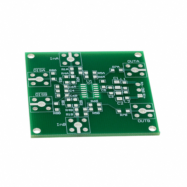
DEM-OPA-SO-1B
BOARD DEMO FOR SNGL 8SOIC OPAMPS
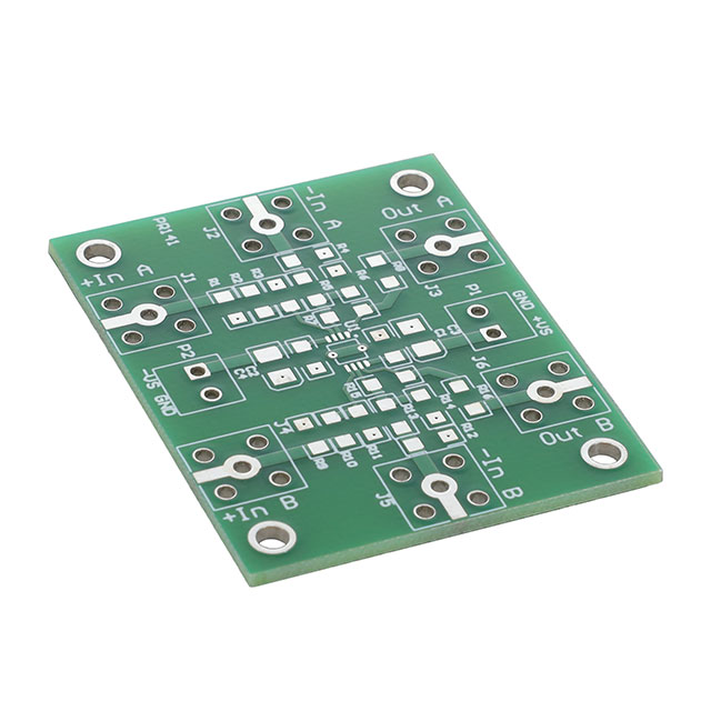
DEM-OPA-SSOP-3E
UNPOPULATED DEMO BOARD
DEM-OPA-SO-3A
DEM-OPA-SO-3A
DEM-OPA-SO-2D
BOARD DEMO FOR 14SOIC DUAL OPAMP
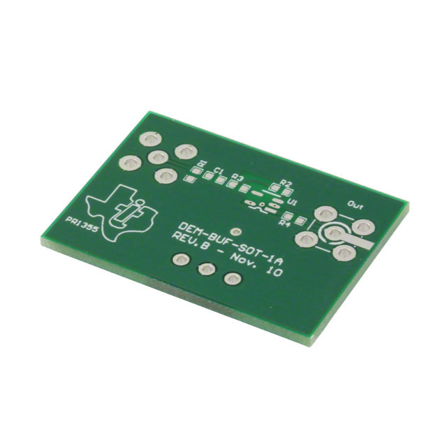
DEM-BUF-SOT-1A
DEM-BUF-SOT-1A
DEM-OPA-MSOP-2A
BOARD DEMO FOR 8MSOP DUAL OPAMPS
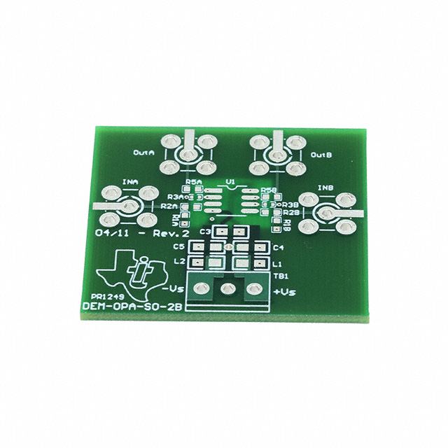
DEM-OPA-SO-2B
BOARD DEMO FOR 8SOIC DUAL OPAMPS
DEM-VCA-MSOP-1A
DEM-VCA-MSOP-1A
DEM-VCA-SO-1B
DEM-VCA-SO-1B
45
Serves customers in 45 countries
1000+
Worldwide Manufacturers
$140M
$140M Growth in 5 Years
50.0M+
50M Parts Shipped in 5 Years