
$4.84
Quantity Available:
1992
SZC Quality Assurance


Texas Instruments
Texas Instruments Incorporated (TI) is a global semiconductor powerhouse, crafts advanced analog ICs and embedded processors. Fueled by top-tier minds, TI's innovations drive tech's future, impacting 100,000+ clients.
View All Product from Texas Instruments


TVP5147PFPR Functional Description
2.1Analog Processing and A/D ConvertersFigure 2−1 shows a functional diagram of the analog processors and A/D converters, which provide the analoginterface to all video inputs. It accepts up to 10 inputs and performs source selection, video clamping, videoamplification, A/D conversion, and gain and offset adjustments to center the digitized video signal. TheTVP5147 supports one analog video output for the selected analog input video.ClampCH1 A/DLine-LockedSampling ClockVI_4_AMUXVI_1_BVI_1_CMUXVI_2_AVI_2_BVI_2_CMUXVI_3_AVI_3_BVI_3_C11-BitADCClampClampClampVI_1_AI/OPGACVBS/Pb/CCVBS/YCVBS/Pr/CCVBS/YMUXPGACH2 A/D11-BitADCPGAAnalog Front EndFigure 2−1. Analog Processors and A/D Converters2.1.1 Video Input Switch ControlThe TVP5147 decoder has two analog channels that accept up to 10 video inputs. The user can configurethe internal analog video switches via the I2C interface. The 10 analog video inputs can be used for differentinput configurations, some of which are:Functional Description10SLES099A—April 2004TVP5147PFP
•Up to 10 selectable individual composite video inputs
•Up to four selectable S-video inputs
•Up to three selectable analog YPbPr video inputs and one CVBS input
•Up to two selectable analog YPbPr video inputs, two S-video inputs, and two CVBS inputsThe input selection is performed by the input select register at I2C subaddress 00h (see Section 2.11.1).2.1.2 Analog Input ClampingAn internal clamping circuit restores the ac-coupled video signal to a fixed dc level. The clamping circuitprovides line-by-line restoration of the video sync level to a fixed dc reference voltage. The selection betweenbottom and mid clamp is performed automatically by the TVP5147 decoder.2.1.3 Automatic Gain ControlThe TVP5147 decoder uses two programmable gain amplifiers (PGAs), one per channel. The PGA can scalea signal with a voltage-input compliance of 0.5-VPP to 2.0-VPP to a full-scale 10-bit A/D output code range.A 4-bit code sets the coarse gain with individual adjustment per channel. Minimum gain corresponds to a code0x0 (2.0-VPP full-scale input, −6-dB gain) while maximum gain corresponds to code 0xF (0.5 VPP full scale,+6-dB gain). The TVP5147 decoder also has 12-bit fine gain controls for each channel and appliesindependently to coarse gain controls. For composite video, the input video signal amplitude can varysignificantly from the nominal level of 1 VPP. The TVP5147 decoder can adjust its PGA setting automatically:an automatic gain control (AGC) can be enabled and can adjust the signal amplitude such that the maximumrange of the ADC is reached without clipping. Some nonstandard video signals contain peak white levels thatsaturate the ADC. In these cases, the AGC automatically cuts back gain to avoid clipping. If the AGC is on,then the TVP5147 decoder can read the gain currently being used.The TVP5147 AGC comprises the front-end AGC before Y/C separation and the back-end AGC after Y/Cseparation. The back-end AGC restores the optimum system gain whenever an amplitude reference such asthe composite peak (which is only relevant before Y/C separation) forces the front-end AGC to set the gaintoo low. The front-end and back-end AGC algorithms can use up to four amplitude references: sync height,color burst amplitude, composite peak, and luma peak.The specific amplitude references being used by the front-end and back-end AGC algorithms can beindependently controlled using the AGC white peak processing register located at subaddress 74h. TheTVP5147 gain increment speed and gain increment delay can be controlled using the AGC increment speedregister located at subaddress 78h and the AGC increment delay register located at subaddress 79h.2.1.4 Analog Video OutputOne of the analog input signals is available at the analog video output terminal, which is shared with inputselected by I2C registers. The signal at this terminal must be buffered by a source follower. The nominal outputvoltage is 2 V p-p, thus the signal can be used to drive a 75-Ω line. The magnitude is maintained with an AGCin 16 steps controlled by the TVP5147 decoder. In order to use this function, terminal VI_1_A must be set asan output terminal. The input mode selection register also selects an active analog output signal.2.1.5 A/D ConvertersAll ADCs have a resolution of 10 bits and can operate up to 30 MSPS. All A/D channels receive an identicalclock from the on-chip phase-locked loop (PLL) at a frequency between 24 MHz and 30 MHz. All ADCreference voltages are generated internally.Functional Description11SLES099A—April 2004TVP5147PFP2.2Digital Video ProcessingFigure 2−2 is a block diagram of the TVP5147 digital video decoder processing. This block receives digitizedvideo signals from the ADCs and performs composite processing for CVBS and S-video inputs and YCbCrsignal enhancements for CVBS and S-video inputs. It also generates horizontal and vertical syncs and otheroutput control signals such as genlock for CVBS and S-video inputs. Additionally, it can provide fieldidentification, horizontal and vertical lock, vertical blanking, and active video window indication signals. Thedigital data output can be programmed to two formats: 20-bit 4:2:2 with external syncs or 10-bit 4:2:2 withembedded/separate syncs. The circuit detects pseudosync pulses, AGC pulses, and color striping inMacrovision-encoded copy-protected material. Information present in the VBI interval can be retrieved andeither inserted in the ITU-R BT.656 output as ancillary data or stored in internal FIFO and/or registers forretrieval via the host port interface.CopyProtectionDetectorVBI DataProcessorOutputFormatterCompositeProcessorCVBS/YC/CbCrYCbCrY[9:0]TimingProcessorAVIDFIDGLCOXTAL1XTAL2RESETBCH1 A/DCH2 A/DHS/CSVS/VBLKDATACLKC[9:0]HostInterfaceSCLSDASlice VBI Data2×DecimationPWDN2×DecimationFigure 2−2. Digital Video Processing Block Diagram2.2.1 2× Decimation FilterAll input signals are typically oversampled by a factor of 2 (27 MHz). The A/D outputs initially pass throughdecimation filters that reduce the data rate to 1× the pixel rate. The decimation filter is a half-band filter.Oversampling and decimation filtering can effectively increase the overall signal-to-noise ratio by 3 dB.2.2.2 Composite ProcessorFigure 2−3 is a block diagram of the TVP5147 digital composite video processing circuit. This processingcircuit receives a digitized composite or S-video signal from the ADCs and performs Y/C separation (bypassedfor S-video input), chroma demodulation for PAL/NTSC and SECAM, and YUV signal enhancements.Functional Description12SLES099A—April 2004TVP5147PFPThe 10-bit composite video is multiplied by the subcarrier signals in the quadrature demodulator to generatecolor difference signals U and V. The U and V signals are then sent to low-pass filters to achieve the desiredbandwidth. An adaptive 5-line comb filter separates UV from Y based on the unique property of color phaseshifts from line to line. The chroma is remodulated through a quadrature modulator and subtracted fromline-delayed composite video to generate luma. This form of Y/C separation is completely complementary,thus there is no loss of information. However, in some applications, it is desirable to limit the U/V bandwidthto avoid crosstalk. In that case, notch filters can be turned on. To accommodate some viewing preferences,a peaking filter is also available in the luma path. Contrast, brightness, sharpness, hue, and saturation controlsare programmable through the host port.LineDelay–PeakingNTSC/PALRemodulationNTSC/PALDemodulationNotchFilterColor LPF↓ 25-LineAdaptiveCombFilterNotchFilterNotchFilterNotchFilterContrastBrightnessSaturationAdjustCrYCbYBurstAccumulator(U)USECAMColorDemodulationVDelayCVBS/YSECAM LumaCVBSCVBS/CColor LPF↓ 2BurstAccumulator(V)UVDelayDelayFigure 2−3. Composite and S-Video Processing Block Diagram2.2.2.1Color Low-Pass FilterHigh filter bandwidth preserves sharp color transitions and produces crisp color boundaries. However, fornonstandard video sources that have asymmetrical U and V side bands, it is desirable to limit the filterbandwidth to avoid UV crosstalk. The color low-pass filter bandwidth is programmable to enable one of thethree notch filters. Figure 2−4 through Figure 2−7 represent the frequency responses of the wideband colorlow-pass filters.Functional Description13SLES099A—April 2004TVP5147PFPFigure 2−4. Color Low-Pass Filter FrequencyResponseFigure 2−5. Color Low-Pass Filter With FilterFrequency Response, NTSC Square PixelSamplingf − Frequency − MHz−70−60−50−40−30−20−100100.00.51.01.52.02.53.03.54.0PAL SQP −3 dB@ 1.55 MHzNTSC SQP −3 dB@ 1.29 MHzITU-R BT.601 −3 dB@ 1.42 MHzAmplitude − dBf − Frequency − MHz−70−60−50−40−30−20−100100.00.51.01.52.02.53.03.54.0Amplitude − dBFilter 0−3 dB @ 1.29 MHzFilter 1−3 dB@ 936 kHzFilter 3−3 dB @ 504 kHzFilter 2−3 dB @ 767 kHz−70−60−50−40−30−20−100100.00.51.01.52.02.53.03.54.0Figure 2−6. Color Low-Pass Filter With FilterCharacteristics, NTSC/PAL ITU-R BT.601SamplingFigure 2−7. Color Low-Pass Filter With FilterCharacteristics, PAL Square Pixel Samplingf − Frequency − MHz−70−60−50−40−30−20−100100.00.51.01.52.02.53.03.54.0Amplitude − dBFilter 3−3 dB @ 554 kHzFilter 2−3 dB @ 844 kHzFilter 1−3 dB@ 1.03 MHzFilter 0−3 dB @ 1.41 MHzf − Frequency − MHzAmplitude − dBFilter 3−3 dB@ 605 kHzFilter 0−3 dB @ 1.55 MHzFilter 2−3 dB @ 922 kHzFilter 1−3 dB@ 1.13 MHzFunctional Description14SLES099A—April 2004TVP5147PFP2.2.2.2Y/C SeparationY/C separation can be done using adaptive 5-line (5-H delay) comb filters or a chroma trap filter. The combfilter can be selectively bypassed in the luma or chroma path. If the comb filter is bypassed in the luma path,then chroma trap filters are used which are shown in Figure 2−8 through Figure 2−11. TI’s patented adaptivecomb filter algorithm reduces artifacts such as hanging dots at color boundaries. It detects and properlyhandles false colors in high-frequency luminance images such as a multiburst pattern or circle pattern.−40−35−30−25−20−15−10−5051001234567f − Frequency − MHzNo Notch FilterNotch 2 FilterAmplitude − dBFigure 2−8. Chroma Trap Filter FrequencyResponse, NTSC Square Pixel SamplingNotch 1 Filterf − Frequency − MHz−40−35−30−25−20−15−10−5051001234567No Notch FilterNotch 3 FilterNotch 1 FilterAmplitude − dBFigure 2−9. Chroma Trap Filter FrequencyResponse, NTSC ITU-R BT.601 SamplingNotch 2 FilterNotch 3 Filter−40−35−30−25−20−15−10−5051001234567f − Frequency − MHz−40−35−30−25−20−15−10−5051001234567Amplitude − dBFigure 2−10. Chroma Trap Filter FrequencyResponse, PAL ITU-R BT.601 SamplingFigure 2−11. Chroma Trap Filter FrequencyResponse, PAL Square Pixel Samplingf − Frequency − MHzAmplitude − dBNo Notch FilterNotch 2 FilterNotch 1 FilterNotch 3 FilterNo Notch FilterNotch 2 FilterNotch 1 FilterNotch 3 FilterFunctional Description15SLES099A—April 2004TVP5147PFP2.2.3 Luminance ProcessingThe digitized composite video signal passes through either a luminance comb filter or a chroma trap filter,either of which removes chrominance information from the composite signal to generate a luminance signal.The luminance signal is then fed into the input of a peaking circuit. Figure 2−12 illustrates the basic functionsof the luminance data path. In the case of S-video, the luminance signal bypasses the comb filter or chromatrap filter and is fed directly to the circuit. A peaking filter (edge enhancer) amplifies high-frequencycomponents of the luminance signal. Figure 2−13, Figure 2−14, and Figure 2−15 show the characteristics ofthe peaking filter at four different gain settings that are user-programmable via the I2C interface.BandpassFilter×GainPeakingFilterIN+OUTDelayPeakDetectorFigure 2−12. Luminance Edge-Enhancer Peaking Block Diagramf − Frequency − MHz−10123456701234567Gain = 0Gain = 2Gain = 1Gain = 0.5Peak atf = 2.40 MHzAmplitude − dBf − Frequency − MHz−10123456701234567Gain = 0Gain = 2Gain = 1Gain = 0.5Peak atf = 2.64 MHzAmplitude − dBFigure 2−13. Peaking Filter Response, NTSCSquare Pixel SamplingFigure 2−14. Peaking Filter Response,NTSC/PAL ITU-R BT.601 SamplingFunctional Description16SLES099A—April 2004TVP5147PFPf − Frequency − MHz−10123456701234567Gain = 0Gain = 2Peak atf = 2.89 MHzGain = 0.5Gain = 1Amplitude − dBFigure 2−15. Peaking Filter Response, PAL Square Pixel Sampling2.2.3.1Color Transient ImprovementColor transient improvement (CTI) enhances horizontal color transients. The color difference signal transitionpoints are maintained, but the edges are enhanced for signals which have bandwidth-limited colorcomponents.2.3Clock CircuitsAn internal line-locked PLL generates the system and pixel clocks. A 14.318-MHz clock is required to drivethe PLL. This can be input to the TVP5147 decoder at the 1.8-V level on terminal 74 (XTAL1), or a crystal of14.318-MHz fundamental resonant frequency can be connected across terminals 74 and 75 (XTAL2). If aparallel resonant circuit is used as shown in Figure 2−16, then the external capacitors must have the followingrelationship:CL1 = CL2 = 2CL − CSTRAY,where CSTRAY is the terminal capacitance with respect to ground. Figure 2−16 shows the reference clockconfigurations. The TVP5147 decoder generates the DATACLK signal used for clocking data.TVP514774XTAL114.318-MHzCrystal75XTAL2TVP514774XTAL175XTAL2CL1CL214.318-MHzClockFigure 2−16. Reference Clock ConfigurationsFunctional Description17SLES099A—April 2004TVP5147PFP2.4Real-Time Control (RTC)Although the TVP5147 decoder is a line-locked system, the color burst information is used to determineaccurately the color subcarrier frequency and phase. This ensures proper operation with nonstandard videosignals that do not follow exactly the required frequency multiple between color subcarrier frequency and videoline frequency. The frequency control word of the internal color subcarrier PLL and the subcarrier reset bit aretransmitted via terminal 37 (GLCO) for optional use in an end system (for example, by a video encoder). Thefrequency control word is a 23-bit binary number. The instantaneous frequency of the color subcarrier can becalculated using the following equation:FPLL �Fctrl223 � Fsclkwhere FPLL is the frequency of the subcarrier PLL, Fctrl is the 23-bit PLL frequency control word, and Fsclk istwo times the pixel frequency. This information can be generated on the GLCO terminal. Figure 2−17 showsthe detailed timing diagram.RTC45 CLK18 CLKLSB03 CLK128 CLK23-Bit Fsc PLL IncrementStartBit1 CLKRSInvalidSampleValidSampleMSB22ReservedNOTE: RTC reset bit (R) is active-low, Sequence bit (S) PAL: 1 = (R-Y) line normal, 0 = (R-Y) line inverted, NTSC: 1 = no changeFigure 2−17. RTC Timing2.5Output FormatterThe output formatter sets how the data is formatted for output on the TVP5147 output buses. Table 2−1 showsthe available output modes.Functional Description18SLES099A—April 2004TVP5147PFPTable 2−1. Output FormatTERMINALNAMETERMINALNUMBER10-Bit 4:2:2YCbCr20-Bit 4:2:2YCbCrY_943Cb9, Y9, Cr9Y9Y_844Cb8, Y8, Cr8Y8Y_745Cb7, Y7, Cr7Y7Y_646Cb6, Y6, Cr6Y6Y_547Cb5, Y5, Cr5Y5Y_450Cb4, Y4, Cr4Y4Y_351Cb3, Y3, Cr3Y3Y_252Cb2, Y2, Cr2Y2Y_153Cb1, Y1, Cr1Y1Y_054Cb0, Y0, Cr0Y0C_957Cb9, Cr9C_858Cb8, Cr8C_759Cb7, Cr7C_660Cb6, Cr6C_563Cb5, Cr5C_464Cb4, Cr4C_365Cb3, Cr3C_266Cb2, Cr2C_169Cb1, Cr1C_070Cb0, Cr0Table 2−2. Summary of Line Frequencies, Data Rates, and Pixel/Line CountsSTANDARDSPIXELS PERLINEACTIVE PIXELSPER LINELINES PERFRAMEPIXELFREQUENCY(MHz)COLORSUBCARRIERFREQUENCY (MHz)HORIZONTALLINE RATE (kHz)601 samplingNTSC-J, M85872052513.53.57954515.73426NTSC-4.4385872052513.54.4336187515.73426PAL-M85872052513.53.5756114915.73426PAL-6085872052513.54.4336187515.73426PAL-B, D, G, H, I86472062513.54.4336187515.625PAL-N86472062513.54.4336187515.625PAL-Nc86472062513.53.5820562515.625SECAM86472062513.5Dr = 4.406250Db = 4.25000015.625Square samplingNTSC-J, M78064052512.27273.57954515.73426NTSC-4.4378064052512.27274.4336187515.73426PAL-M78064052512.27273.5756114915.73426PAL-6078064052512.27274.4336187515.73426PAL-B, D, G, H, I94476862514.754.4336187515.625PAL-N94476862514.754.4336187515.625PAL-Nc94476862514.753.5820562515.625SECAM94476862514.75Dr = 4.406250Db = 4.25000015.625Functional Description19SLES099A—April 2004TVP5147PFP2.5.1 Separate SyncsVS, HS, and VBLK are independently software programmable to a 1× pixel count. This allows any possiblealignment to the internal pixel count and line count. The default settings for 525-line and 625-line video outputsare given as examples below. FID changes at the same transient time when the trailing edge of vertical syncoccurs. The polarity of FID is programmable by an I2C interface.First Field Video525VSVBLKFID123456789102021525-LineHSVS StartVS StopCSVBLK StartVBLK StopSecond Field Video262VSVBLKFID263264265266267268269270271272273283284HSVS StartVS StopCSVBLK StartVBLK StopNOTE: Line numbering conforms to ITU-R BT.470Figure 2−18. Vertical Synchronization Signals for 525-Line SystemFunctional Description20SLES099A—April 2004TVP5147PFPFirst Field VideoVSVBLKFID625-LineHSVS StartVS StopCSVBLK StartVBLK StopSecond Field Video310VSVBLKFID311312313314315316317318319320336337HSVS StartVS StopCSVBLK StartVBLK Stop6226236246251234567232425338NOTE: Line numbering conforms to ITU-R BT.470Figure 2−19. Vertical Synchronization Signals for 625-Line SystemFunctional Description21SLES099A—April 2004TVP5147PFPY[9:0]NTSC 601106PAL 601DATACLK = 2× Pixel ClockNTSC SqpPAL Sqp11210814412812812812842484480ModeABC276288280352DCbDATACLKEAV1YCrYEAV2EAV3EAV4SAV1SAV2SAV3SAV4Cb0Y0Cr0Y10HS StartHorizontal BlankingHSHS StopACBAVIDDAVID StopAVID StartNOTE: ITU-R BT.656 10-bit 4:2:2 timing with 2× pixel clock referenceFigure 2−20. Horizontal Synchronization Signals for 10-Bit 4:2:2 ModeFunctional Description22SLES099A—April 2004TVP5147PFPCbCr[9:0]NTSC 60153PAL 601DATACLK = 1× Pixel ClockNTSC SqpPAL Sqp5654726464646419222038ModeABC136142138174DCbDATACLKCrCbCrCb0 Cr0Cb1Cr10HS StartHorizontal BlankingHSHS StopACBAVIDDNOTE: AVID rising edge occurs 4 clock cycles early.Y[9:0]YYYYY0Y1Y2Y3Horizontal Blanking2AVID StopAVID StartNOTE: 20-bit 4:2:2 timing with 1× pixel clock referenceFigure 2−21. Horizontal Synchronization Signals for 20-Bit 4:2:2 ModeFunctional Description23SLES099A—April 2004TVP5147PFPNTSC 60164PAL 60110-Bit (PCLK = 2× Pixel Clock)NTSC SqpPAL Sqp646464ModeB/2First FieldB/2858864780944H/23220-Bit (PCLK = 1× Pixel Clock)323232B/2429432390472H/2HSVSSecond FieldHSVSB/2H/2 + B/2H/2 + B/2Figure 2−22. VSYNC Position With Respect to HSYNC2.5.2 Embedded SyncsStandards with embedded syncs insert the SAV and EAV codes into the data stream on the rising and fallingedges of AVID. These codes contain the V and F bits which also define vertical timing. Table 2−3 gives theformat of the SAV and EAV codes.H equals 1 always indicates EAV. H equals 0 always indicates SAV. The alignment of V and F to the line andfield counter varies depending on the standard.The P bits are protection bits:P3 = V xor H; P2 = F xor H; P1 = F xor V; P0 = F xor V xor HTable 2−3. EAV and SAV SequenceD9 (MSB)D8D7D6D5D4D3D2D1D0Preamble1111111111Preamble0000000000Preamble0000000000Status word1FVHP3P2P1P0002.6I2C Host InterfaceCommunication with the TVP5147 decoder is via an I2C host interface. The I2C standard consists of twosignals, the serial input/output data (SDA) line and the serial input clock line (SCL), which carry informationbetween the devices connected to the bus. A third signal (I2CA) is used for slave address selection. Althoughan I2C system can be multimastered, the TVP5147 decoder functions as a slave device only.Functional Description24SLES099A—April 2004TVP5147PFPBecause SDA and SCL are kept open-drain at a logic-high output level or when the bus is not driven, the usermust connect SDA and SCL to a positive supply voltage via a pullup resistor on the board. The slave addressesselect signal, terminal 37 (I2CA), enables the use of two TVP5147 devices tied to the same I2C bus, becauseit controls the least significant bit of the I2C device address.Table 2−4. I2C Host Interface Terminal DescriptionSIGNALTYPEDESCRIPTIONI2CAISlave address selectionSCLIInput clock lineSDAI/OInput/output data line2.6.1 Reset and I2C Bus Address SelectionThe TVP5147 decoder can respond to two possible chip addresses. The address selection is made at resetby an externally supplied level on the I2CA terminal. The TVP5147 decoder samples the level of terminal 37at power up or at the trailing edge of RESETB and configures the I2C bus address bit A0. The I2CA terminalhas an internal pulldown resistor to pull the terminal low to set a zero.Table 2−5. I2C Address SelectionA6A5A4A3A2A1A0 (I2CA)R/WHEX1011100 (default)1/0B9/B81011101 †1/0BB/BA† If terminal 37 is strapped to DVDD via a 2.2-kΩ resistor, I2C device address A0 is set to 1.2.6.2 I2C OperationData transfers occur using the following illustrated formats.S10111000ACKSubaddressACKSend dataACKPRead from I2C control registersS10111000ACKSubaddressACKS10111001ACKReceive dataNAKPS = I2C bus start conditionP = I2C bus stop conditionACK = Acknowledge generated by the slaveNAK = Acknowledge generated by the master, for multiple-byte read master with ACK each byte exceptlast byteSubaddress = Subaddress byteData = Data byte. If more than one byte of data is transmitted (read and write), the subaddress pointer isautomatically incremented.I2C bus address = Example shown that I2CA is in default mode. Write (B8h), read (B9h)2.6.3 VBUS AccessThe TVP5147 decoder has additional internal registers accessible through an indirect access to an internal24-bit address wide VBUS. Figure 2−23 shows the VBUS register access.Functional Description25SLES099A—April 2004TVP5147PFPSingle ByteB8SACKE8ACKVA0ACKVA1ACKVA2ACKPVBUS WriteB8SACKE0ACKSend DataACKPMultiple BytesB8SACKE8ACKVA0ACKVA1ACKVA2ACKPB8SACKE1ACKSend DataACKACKPSend Data
•
•
•Single ByteB8SACKE8ACKVA0ACKVA1ACKVA2ACKPVBUS ReadB8SACKE0ACKACKMultiple BytesB8SACKE8ACKVA0ACKVA1ACKVA2ACKPB8SACKE1ACKACKNAKPRead Data
•
•
•Read DataNAKPSB9SB9ACKRead DataHOSTProcessorI2CVBUSDataI2C Registers00hE0hE1hVBUSAddressE8hEAhFFhVBUS[23:0]LineModeVBUS Registers00 0000hFIFOVPSVITCWSSCC80 051Ch80 0520h80 052Ch80 0600h80 0700h90 1904hFF FFFFhNOTE: Examples use default I2C addressACK = Acknowledge generated by the slaveNAK = No acknowledge generated by the masterFigure 2−23. VBUS AccessFunctional Description26SLES099A—April 2004TVP5147PFP2.7VBI Data ProcessorThe TVP5147 VBI data processor (VDP) slices various data services like teletext (WST, NABTS), closedcaption (CC), wide screen signaling (WSS), program delivery control (PDC), vertical interval time code (VITC),video program system (VPS), copy generation management system (CGMS) data, and electronic programguide (Gemstar) 1x/2x. Table 2−6 shows the supported VBI system.These services are acquired by programming the VDP to enable the reception of one or more vertical blankinterval (VBI) data standard(s) during the VBI. The VDP can be programmed on a line-per-line basis to enablesimultaneous reception of different VBI formats, one per line. The results are stored in a FIFO and/or registers.Because of the high data bandwidth, teletext results are stored in FIFO only. The TVP5147 decoder providesfully decoded V-Chip data to the dedicated registers at subaddresses 80 0540h−80 0543h.Table 2−6. Supported VBI SystemVBI SYSTEMSTANDARDLINE NUMBERNUMBER OF BYTESTeletext WST ASECAM6−23 (Fields 1 and 2)38Teletext WST BPAL6−22 (Fields 1 and 2)43Teletext NABTS CNTSC10−21 (Fields 1 and 2)34Teletext NABTS DNTSC-J10−21 (Fields 1 and 2)35Closed CaptionPAL22 (Fields 1 and 2)2Closed CaptionNTSC21 (Fields 1 and 2)2WSSPAL23 (Fields 1 and 2)14 bitsWSS-CGMSNTSC20 (Fields 1 and 2)20 bitsVITCPAL6−229VITCNTSC10−209VPS (PDC)PAL1613V-Chip (decoded)NTSC21 (Fields 1 and 2)2Gemstar 1xNTSC2Gemstar 2xNTSC5 with frame byteUserAnyProgrammableProgrammableFunctional Description27SLES099A—April 2004TVP5147PFP2.7.1 VBI FIFO and Ancillary Data in Video StreamSliced VBI data can be output as ancillary data in the video stream in ITU-R BT.656 mode. VBI data is outputon the Y[9:2] terminals during the horizontal blanking period. Table 2−7 shows the header format andsequence of the ancillary data inserted into the video stream. This format is also used to store any VBI datainto the FIFO. The size of the FIFO is 512 bytes. Therefore, the FIFO can store up to 11 lines of teletext datawith the NTSC NABTS standard.Table 2−7. Ancillary Data Format and SequenceBYTENO.D7(MSB)D6D5D4D3D2D1D0(LSB)DESCRIPTION000000000111111111Ancillary data preamble211111111Ancillary data preamble3NEPEP010DID2DID1DID0Data ID (DID)4NEPEPF5F4F3F2F1F0Secondary data ID (SDID)5NEPEPN5N4N3N2N1N0Number of 32-bit data (NN)6Video line # [7:0]Internal data ID0 (IDID0)7000DataerrorMatch#1Match#2Video line # [9:8]Internal data ID1 (IDID1)81. DataData byte1st word92. DataData byte1 word103. DataData byte114. DataData byte::::m. DataData byteNth wordCS[7:0]Check sumNword4N+700000000Fill byteNOTE: The number of bytes (m) varies depending on the VBI data service.EP:Even parity for D0−D5, NEP: Negated even parityDID:91h: Sliced data of VBI lines of first field53h: Sliced data of line 24 to end of first field55h: Sliced data of VBI lines of second field97h: Sliced data of line 24 to end of second fieldSDID:This field holds the data format taken from the line mode register bits [2:0] of the corresponding line.NN:Number of Dwords beginning with byte 8 through 4N+7. Note this value is the number of Dwordswhere each Dword is 4 bytes.IDID0:Transaction video line number [7:0]IDID1:Bit 0/1 = Transaction video line number [9:8]Bit 2 = Match 2 flagBit 3 = Match 1 flagBit 4 = 1 if an error was detected in the EDC block. 0 if no error was detected.CS:Sum of D0−D7 of first data through last data byte.Fill byte:Fill bytes make a multiple of 4 bytes from byte 0 to last fill byte. For teletext modes, byte 8 is the syncpattern byte. Byte 9 is the first data byte.Functional Description28SLES099A—April 2004TVP5147PFP2.7.2 VBI Raw Data OutputThe TVP5147 decoder can output raw A/D video data at twice the sampling rate for external VBI slicing. Thisis transmitted as an ancillary data block, although somewhat differently from the way the sliced VBI data istransmitted in the FIFO format as described in Section 2.7.1. The samples are transmitted during the activeportion of the line. VBI raw data uses ITU-R BT.656 format having only luma data. The chroma samples arereplaced by luma samples. The TVP5147 decoder inserts a four-byte preamble 000h 3FFh 3FFh 180h beforedata start. There are no checksum bytes and fill bytes in this mode.Table 2−8. VBI Raw Data Output FormatBYTENO.D9(MSB)D8D7D6D5D4D3D2D1D0(LSB)DESCRIPTION0000000000011111111111VBI raw data preamble21111111111VBI raw data preamble3011000000041. Data52. Data2 pixel rate luma data::2× pixel rate luma data(i.e., NTSC 601: n = 1707)n−1n−5. Data(i.e., NTSC 601: n = 1707)nn–4. Data2.8Reset and InitializationReset is initiated at power up or any time terminal 34 (RESETB) is brought low. Table 2−9 describes the statusof the TVP5147 terminals during and immediately after reset.Table 2−9. Reset SequenceSIGNAL NAMEDURING RESETRESET COMPLETEDY[9:0], C[9:0]InputHigh-impedanceRESETB, PWDN, SDA, SCL, FSS,AVID, GLCO, HS, VS, FIDInputInputINTREQInputOutputDATACLKOutputHigh-impedance200 ns (min)RESETB(Pin 34)1 ms (min)Invalid I2C CycleValidNormal OperationReset1 ms (min)SDA(Pin 29)POWER(3.3 V and 1.8 V)Figure 2−24. Reset TimingThe TVP5147 requires that pin 69 (C_1/GPIO) be held LOW. If using the 20-/16-bit mode or using this pin asGPIO, then this pin must be pulled low through a 2.2-kΩ pulldown resistor (see Figure 5−1). If unused, thispin can be shorted to ground. (Note: If using the 20-/16-bit mode and only using the 16 MSBs, it is possibleto short pin 69 to GND, but the current for IOVDD will increase by 2 or 3 mA.)Functional Description29SLES099A—April 2004TVP5147PFPAfter reset, the user must write the following I2C commands to the TVP5147:STEPI2C SUBADDRESSI2C DATA10xE80x0220xE90x0030xEA0x8040xE00x0150xE80x6060xE90x0070xEA0xB080xE00x0190xE80x16100xE90x00110xEA0xA0120xE00x16130xE80x60140xE90x00150xEA0xB0160xE00x00Afterward, the user programs the device as usual.2.9Adjusting External SyncsThe proper sequence to program the following external syncs is:
•To set NTSC, PAL-M, NTSC 443, PAL60 (525-line modes):−Set the video standard to NTSC (register 02h)−Set HSYNC, VSYNC, VBLK, and AVID external syncs (registers 16h through 24h)
•To set PAL, PAL-N, SECAM (625-line modes):−Set the video standard to PAL (register 02h)−Set HSYNC, VSYNC, VBLK, and AVID external syncs (registers 16h through 24h)
•For autoswitch, set the video standard to autoswitch (register 02h)2.10 Internal Control RegistersThe TVP5147 decoder is initialized and controlled by a set of internal registers that define the operatingparameters of the entire device. Communication between the external controller and the TVP5147 is througha standard I2C host port interface, as described earlier. Table 2−10 shows the summary of these registers.Detailed programming information for each register is described in the following sections. Additional registersare accessible through an indirect procedure involving access to an internal 24-bit address wide VBUS.Table 2−11 shows the summary of the VBUS registers.NOTE: Do not write to reserved registers. Reserved bits in any defined register must be writtenwith 0s, unless otherwise noted.Functional Description30SLES099A—April 2004TVP5147PFPTable 2−10. I2C Register SummaryREGISTER NAMEI2C SUBADDRESSDEFAULTR/WInput select00h00hR/WAFE gain control01h0FhR/WVideo standard02h00hR/WOperation mode03h00hR/WAutoswitch mask04h23hR/WColor killer05h10hR/WLuminance processing control 106h00hR/WLuminance processing control 207h00hR/WLuminance processing control 308h02hR/WLuminance brightness09h80hR/WLuminance contrast0Ah80hR/WChrominance saturation0Bh80hR/WChroma hue0Ch00hR/WChrominance processing control 10Dh00hR/WChrominance processing control 20Eh0EhR/WReserved0Fh−15hAVID start pixel16h−17h055hR/WAVID stop pixel18h−19h325hR/WHSYNC start pixel1Ah−1Bh000hR/WHSYNC stop pixel1Ch−1Dh040hR/WVSYNC start line1Eh−1Fh004hR/WVSYNC stop line20h−21h007hR/WVBLK start line22h−23h001hR/WVBLK stop line24h−25h015hR/WReserved26h−2AhOverlay delay2Bh00hR/WReserved2ChCTI delay2Dh00hR/WCTI control2Eh00hR/WReserved2Fh−30hGLCO/RTC31h05hR/WSync control32h00hR/WOutput formatter 133h40hR/WOutput formatter 234h00hR/WOutput formatter 335hFFhR/WOutput formatter 436hFFhR/WOutput formatter 537hFFhR/WOutput formatter 638hFFhR/WClear lost lock detect39h00hR/WStatus 13AhRStatus 23BhRNOTE: R = Read onlyW = Write onlyR/W = Read and writeReserved register addresses must not be written to.Functional Description31SLES099A—April 2004TVP5147PFPTable 2−10. I2C Register Summary (Continued)REGISTER NAMEI2C SUBADDRESSDEFAULTR/WAGC gain status3Ch−3DhRReserved3EhVideo standard status3FhRGPIO input 140hRGPIO input 241hRVertical line count42h−43hRReserved44h−45hAFE coarse gain for CH146h20hR/WAFE coarse gain for CH247h20hR/WAFE coarse gain for CH348h20hR/WAFE coarse gain for CH449h20hR/WAFE fine gain for Pb4Ah−4Bh900hR/WAFE fine gain for chroma4Ch−4Dh900hR/WAFE fine gain for Pr4Eh−4Fh900hR/WAFE fine gain for CVBS_Luma50h−51h900hR/WReserved52h−56hField ID control57h00hR/WReserved58h−6FhROM version70hRReserved71h−73hAGC white peak processing74h00hR/WF and V bit control75h12hR/WVCR trick mode control76h8AhR/WHorizontal shake increment77h64hR/WAGC increment speed78h05hR/WAGC increment delay79h1EhR/WReserved7Ah−7EhAnalog output control 17Fh00hR/WChip ID MSB80h51hRChip ID LSB81h47hRReserved82h−B0hVDP TTX filter 1 mask 1B1h00hR/WVDP TTX filter 1 mask 2B2h00hR/WVDP TTX filter 1 mask 3B3h00hR/WVDP TTX filter 1 mask 4B4h00hR/WVDP TTX filter 1 mask 5B5h00hR/WVDP TTX filter 2 mask 1B6h00hR/WVDP TTX filter 2 mask 2B7h00hR/WVDP TTX filter 2 mask 3B8h00hR/WVDP TTX filter 2 mask 4B9h00hR/WVDP TTX filter 2 mask 5BAh00hR/WNOTE: R = Read onlyW = Write onlyR/W = Read and writeReserved register addresses must not be written to.Functional Description32SLES099A—April 2004TVP5147PFPTable 2−10. I2C Register Summary (Continued)REGISTER NAMEI2C SUBADDRESSDEFAULTR/WVDP TTX filter controlBBh00hR/WVDP FIFO word countBChRVDP FIFO interrupt thresholdBDh80hR/WReservedBEhVDP FIFO resetBFh00hR/WVDP FIFO output controlC0h00hR/WVDP line number interruptC1h00hR/WVDP pixel alignmentC2h−C3h01EhR/WReservedC4h−D5hVDP line startD6h06hR/WVDP line stopD7h1BhR/WVDP global line modeD8hFFhR/WVDP full field enableD9h00hR/WVDP full field modeDAhFFhR/WReservedDBh−DFhVBUS data access with no VBUS address incrementE0h00hR/WVBUS data access with VBUS address incrementE1h00hR/WFIFO read dataE2hRReservedE3h−E7hVBUS address accessE8h−EAh00 0000hR/WReservedEBh−EFhInterrupt raw status 0F0hRInterrupt raw status 1F1hRInterrupt status 0F2hRInterrupt status 1F3hRInterrupt mask 0F4h00hR/WInterrupt mask 1F5h00hR/WInterrupt clear 0F6h00hR/WInterrupt clear 1F7h00hR/WReservedF8h−FFhNOTE: R = Read onlyW = Write onlyR/W = Read and writeReserved register addresses must not be written to.Functional Description33SLES099A—April 2004TVP5147PFPTable 2−11. VBUS Register SummaryREGISTER NAMEI2C SUBADDRESSDEFAULTR/WReserved00 0000h−80 051BhVDP closed caption data80 051Ch−80 051FhRVDP WSS data80 0520h−80 0526hRReserved80 0527h−80 052BhVDP VITC data80 052Ch−80 0534hRReserved80 0535h−80 053FhVDP V-Chip data80 0540h−80 0543hRReserved80 0544h−80 05FFhVDP general line mode and line address80 0600h−80 0611h00h, FFhR/WReserved80 0612h−80 06FFhVDP VPS (PDC)/Gemstar data80 0700h−80 070ChRReserved80 070Dh−90 1903hVDP FIFO read90 1904hRReserved90 1905h−A0 005DhAnalog output control 2A0 05EhB2hR/WReservedA0 005Fh−B0 005FhInterrupt configurationB0 0060h00hR/WReservedB0 0061h−FF FFFFhNOTE: Writing any value to a reserved register may cause erroneous operation of the TVP5147 decoder.It is recommended not to access any data to/from reserved registers.Functional Description34SLES099A—April 2004TVP5147PFP2.11 Register Definitions2.11.1Input Select RegisterSubaddress00hDefault00h76543210Input select [7:0]Table 2−12. Analog Channel and Video Mode SelectionMODEINPUT(S) SELECTEDINPUT SELECT [7:0]OUTPUTMODEINPUT(S) SELECTED76543210HEXOUTPUT(see Note 1)CVBSVI_1_A (default)0000000000N/AVI_1_B0000000101VI_1_BVI_1_C0000001002VI_1_CVI_2_A0000010004VI_2_AVI_2_B0000010105VI_2_BVI_2_C0000011006VI_2_CVI_3_A0000100008VI_3_AVI_3_B0000100109VI_3_BVI_3_C000010100AVI_3_CVI_4_A000011000CVI_4_AS-videoVI_2_A(Y), VI_1_A(C)0100010044N/AVI_2_B(Y), VI_1_B(C)0100010145VI_2_B(Y)VI_2_C(Y), VI_1_C(C)0100011046VI_2_C(Y)VI_2_A(Y), VI_3_A(C)0101010054VI_2_A(Y)VI_2_B(Y), VI_3_B(C)0101010155VI_2_B(Y)VI_2_C(Y), VI_3_C(C)0101011056VI_2_C(Y)VI_4_A(Y), VI_1_A(C)010011004CN/AVI_4_A(Y), VI_1_B(C)010011014DVI_4_A(Y)VI_4_A(Y), VI_1_C(C)010011104EVI_4_A(Y)VI_4_A(Y), VI_3_A(C)010111005CVI_4_A(Y)VI_4_A(Y), VI_3_B(C)010111015DVI_4_A(Y)VI_4_A(Y), VI_3_C(C)010111105EVI_4_A(Y)YPbPrVI_1_A(Pb), VI_2_A(Y), VI_3_A(Pr)1001010094N/AVI_1_B(Pb), VI_2_B(Y), VI_3_B(Pr)1001010195VI_2_B(Y)VI_1_C(Pb), VI_2_C(Y), VI_3_C(Pr)1001011096VI_2_C(Y)NOTE 1:When VI_1_A is set to output, the total number of inputs is nine. The video output can be either CVBS or luma.Ten input terminals can be configured to support composite, S-video, and component YPbPr as listed inTable 2−12. User must follow this table properly for S-video and component applications because only theterminal configurations listed in Table 2−12 are supported.Functional Description35SLES099A—April 2004TVP5147PFP2.11.2AFE Gain Control RegisterSubaddress01hDefault0Fh76543210Reserved11AGC chromaAGC lumaBit 3: 1 must be written to this bit.Bit 2: 1 must be written to this bit.AGC chroma enable: Controls automatic gain in the chroma/PbPr channel:0 = Manual (if AGC luma is set to manual, AGC chroma is forced to be in manual)1 = Enabled auto gain, applied a gain value acquired from the sync channel for S-video and componentmode. When AGC luma is set, this state is valid. (default)AGC luma enable: Controls automatic gain in the embedded sync channel of CVBS, S-video, componentvideo:0 = Manual gain, AFE coarse and fine gain frozen to the previous gain value set by AGC when this bit is setto 0.1 = Enabled auto gain applied to only the embedded sync channel (default)These settings only affect the analog front-end (AFE). The brightness and contrast controls are not affectedby these settings.2.11.3Video Standard RegisterSubaddress02hDefault00h76543210ReservedVideo standard [2:0]Video standard [2:0]:CVBS and S-VideoComponent Video000= Autoswitch mode (default)Autoswitch mode (default)001= (M, J) NTSCComponent 525010= (B, D, G, H, I, N) PALComponent 625011= (M) PALReserved100= (Combination-N) PALReserved101= NTSC 4.43Reserved110= SECAMReserved111= PAL 60ReservedWith the autoswitch code running, the user can force the decoder to operate in a particular video standardmode by writing the appropriate value into this register. Changing these bits causes the register settings tobe reinitialized.NOTE: Sampling rate (either square pixel or ITU-R BT.601) can be set by bit 7 (sampling rate)in the output formatter 1 register at I2C subaddress 33h (see Section 2.11.28).Functional Description36SLES099A—April 2004TVP5147PFP2.11.4Operation Mode RegisterSubaddress03hDefault00h76543210ReservedPower down/save [1:0]Power down/save [1:0]:00 = Normal operation (default)01 = Power-save mode. Reduces the clock speed of the internal processor and switches off the ADCs. I2Cinterface is active and all current operating settings are preserved.10 = Reserved11 = Power-down mode. I2C interface does not respond. Turns off all internal clocks and powers down theanalog and digital cores. A hardware reset (RESETB) is required to recover, after which theoperation resumes in the default power-up state.2.11.5Autoswitch Mask RegisterSubaddress04hDefault23h76543210ReservedPAL 60SECAMNTSC 4.43(Nc) PAL(M) PALPAL(M, J) NTSCAutoswitch mode mask: Limits the video formats between which autoswitch is possible.PAL 60:0 = Autoswitch does not include PAL 60 (default)1 = Autoswitch includes PAL60SECAM:0 = Autoswitch does not include SECAM1 = Autoswitch includes SECAM (default)NTSC 4.43:0 = Autoswitch does not include NTSC 4.43 (default)1 = Autoswitch includes NTSC 4.43(Nc) PAL:0 = Autoswitch does not include (Nc) PAL (default)1 = Autoswitch includes (Nc) PAL(M) PAL:0 = Autoswitch does not include (M) PAL (default)1 = Autoswitch includes (M) PALPAL:0 = Reserved1 = Autoswitch includes (B, D, G, H, I, N) PAL (default)(M, J ) NTSC:0 = Reserved1 = Autoswitch includes (M, J) NTSC (default)NOTE: Bits 1 and 0 must always be 1.Functional Description37SLES099A—April 2004TVP5147PFP2.11.6Color Killer RegisterSubaddress05hDefault10h76543210ReservedAutomatic color killerColor killer threshold [4:0]Automatic color killer:00 = Automatic mode (default)01 = Reserved10 = Color killer enabled, the UV terminals are forced to a zero color state.11 = Color killer disabledColor killer threshold [4:0]:1 1111 = 31 (maximum)1 0000 = 16 (default)0 0000 = 0 (minimum)2.11.7Luminance Processing Control 1 RegisterSubaddress06hDefault00h76543210ReservedPedestal not presentReservedVBI rawLuminance signal delay [3:0]Pedestal not present:0 = 7.5 IRE pedestal is present on the analog video input signal (default)1 = Pedestal is not present on the analog video input signalVBI raw:0 = Disabled (default)1 = EnabledDuring the duration of the vertical blanking as defined by the VBLK start and stop line registers atsubaddresses 22h through 25h (see Sections 2.11.22 and 2.11.23), the chroma samples are replaced by lumasamples. This feature can be used to support VBI processing performed by an external device during thevertical blanking interval. In order to use this bit, the output format must be 10-bit ITU-R BT.656 mode.Luminance signal delay [3:0]: Luminance signal delays with respect to the chroma signal in 1× pixel clockincrements.0111 = Reserved0110 = 6-pixel delay0001 = 1-pixel delay0000 = 0 delay (default)1111 = −1-pixel delay1000 = −8-pixel delayFunctional Description38SLES099A—April 2004TVP5147PFP2.11.8Luminance Processing Control 2 RegisterSubaddress07hDefault00h76543210Luma filter select [1:0]ReservedPeaking gain [1:0]ReservedLuma filter selected [1:0]:00 = Luminance adaptive comb enabled (default on CVBS)01 = Luminance adaptive comb disabled (trap filter selected)10 = Luma comb/trap filter bypassed (default on S-video, component mode, and SECAM)11 = ReservedPeaking gain [1:0]:00 = 0 (default)01 = 0.510 = 111 = 22.11.9Luminance Processing Control 3 RegisterSubaddress08hDefault02h76543210ReservedTrap filter select [1:0]Trap filter select [1:0] selects one of the four trap filters to produce the luminance signal by removing thechrominance signal from the composite video signal. The stop band of the chroma trap filter is centered at thechroma subcarrier frequency with the stop-band bandwidth controlled by the two control bits.Trap filter stop-band bandwidth (MHz):Filter select [1:0]NTSC ITU-R BT.601NTSC square pixelPAL ITU-R BT.601PAL square pixel00 =1.21291.10261.21291.325201 =0.87010.79100.87010.950710 = (default)0.71830.67120.73830.806611 =0.50100.45540.50100.54742.11.10Luminance Brightness RegisterSubaddress09hDefault80h76543210Brightness [7:0]Brightness [7:0]: This register works for CVBS, S-video, and component video luminance.1111 1111 = 255 (bright)1000 0000 = 128 (default)0000 0000 = 0 (dark)Functional Description39SLES099A—April 2004TVP5147PFP2.11.11Luminance Contrast RegisterSubaddress0AhDefault80h76543210Contrast [7:0]Contrast [7:0]: This register works for CVBS, S-video, and component video luminance.1111 1111 = 255 (maximum contrast)1000 0000 = 128 (default)0000 0000 = 0 (minimum contrast)2.11.12Chrominance Saturation RegisterSubaddress0BhDefault80h76543210Saturation [7:0]Saturation [7:0]: This register works for CVBS, S-video, and component video luminance.1111 1111 = 255 (maximum)1000 0000 = 128 (default)0000 0000 = 0 (no color)2.11.13Chroma Hue RegisterSubaddress0ChDefault00h76543210Hue [7:0]Hue [7:0] (does not apply to component video)0111 1111 = +180 degrees0000 0000 = 0 degrees (default)1000 0000 = −180 degrees2.11.14Chrominance Processing Control 1 RegisterSubaddress0DhDefault00h76543210ReservedColor PLL resetChrominance adaptivecomb enableReservedAutomatic color gain control [1:0]Color PLL reset:0 = Color subcarrier PLL not reset (default)1 = Color subcarrier PLL resetChrominance adaptive comb enable: This bit is effective on composite video only.0 = Enabled (default)1 = DisabledAutomatic color gain control (ACGC) [1:0]:00= ACGC enabled (default)01 = Reserved10= ACGC disabled, ACGC set to the nominal value11= ACGC frozen to the previous set valueFunctional Description40SLES099A—April 2004TVP5147PFP2.11.15Chrominance Processing Control 2 RegisterSubaddress0EhDe
Product Attributes
| TYPE | DESCRIPTION | Select all |
|---|---|---|
| Type | Video Decoder | |
| Product Status | Not For New Designs | |
| Package | Tape & Reel (TR) | |
| Series | - | |
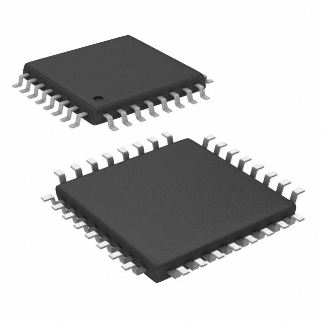
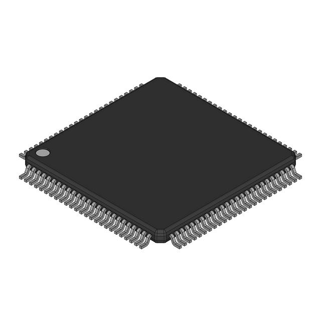
| Supplier Device Package | 80-HTQFP (12x12) | |
| Package / Case | 80-TQFP Exposed Pad | |
| Mounting Type | Surface Mount | |
| Voltage - Supply, Digital | 1.8V, 3.3V | |
| Voltage - Supply, Analog | 1.8V, 3.3V | |
| Applications | LCD TV/Monitor |
$4.84
Quantity Available:
1992
SZC Quality Assurance
Texas Instruments
Texas Instruments Incorporated (TI) is a global semiconductor powerhouse, crafts advanced analog ICs and embedded processors. Fueled by top-tier minds, TI's innovations drive tech's future, impacting 100,000+ clients.
View All Product from Texas InstrumentsYou May Also Be Interested In
More Electronic Parts MoreTVP5147PFPR
IC VIDEO DECODER 10BIT 80TQFP
JM38510/33702B2A
DECIDER, DUAL 2-TO-4 LINE
TVP5151IPBSR
IC VIDEO DECODER 32TQFP
TVP5158IPNPR
IC DECOD VIDEO PAL/NTSC 128HTQFP
TVP5150AM1IPBS
IC VIDEO DECODER 9BIT 32TQFP
TVP5150AM1PBSR
IC DECODER VIDEO DIGITAL 32-TQFP
TVP5151PBSR
IC VIDEO DECODER 32TQFP
TVP5150PBS
IC NTSC/PAL/SECAM DECODER 32TQFP

TVP5154AIPNP
IC VIDEO DECODER 4CH 128-HTQFP
TMS320AV410PJM
COLOR SIGNAL ENCODER,
45
Serves customers in 45 countries
1000+
Worldwide Manufacturers
$140M
$140M Growth in 5 Years
50.0M+
50M Parts Shipped in 5 Years