


$2.77
Price update:a months ago
Available in stock:
2035


45
Serves customers in 45 countries
1000+
Worldwide Manufacturers
$140M
$140M Growth in 5 Years
50.0M+
50M Parts Shipped in 5 Years

Lattice Semiconductor Corporation
Lattice Semiconductor leads in low-power programmability, solving complex challenges across networks, from Edge to Cloud. With a foothold in communication, computing, industry, autos, and consumers, they nurture lasting relationships, offering world-class support for unfettered innovation, crafting a secure, connected world.
View All Product from Lattice Semiconductor Corporation


The LatticeECP/EC family of FPGA devices has been optimized to deliver mainstream FPGA features at low cost. For maximum performance and value, the LatticeECP (EConomy Plus) FPGA concept combines an efficient FPGA fabric with high-speed dedicated functions. Lattice’s first family to implement this approach is the LatticeECP-DSP (EConomy Plus DSP) family, providing dedicated high-performance DSP blocks on-chip. The LatticeEC™ (EConomy) family supports all the general purpose features of LatticeECP devices without dedicated function blocks to achieve lower cost solutions.
The LatticeECP/EC FPGA fabric, which was designed from the outset with low cost in mind, contains all the critical FPGA elements: LUT-based logic, distributed and embedded memory, PLLs and support for mainstream I/Os. Dedicated DDR memory interface logic is also included to support this memory that is becoming increasingly prevalent in cost-sensitive applications.
The ispLEVER® design tool from Lattice allows large complex designs to be efficiently implemented using the LatticeECP/EC family of FPGA devices. Synthesis library support for LatticeECP/EC is available for popular logic synthesis tools. The ispLEVER tool uses the synthesis tool output along with the constraints from its floor planning tools to place and route the design in the LatticeECP/EC device. The ispLEVER tool extracts the timing from the routing and back-annotates it into the design for timing verification.
Lattice provides many pre-designed IP (Intellectual Property) ispLeverCORE™ modules for the LatticeECP/EC family. By using these IPs as standardized blocks, designers are free to concentrate on the unique aspects of their design, increasing their productivity.
Feature
■ Extensive Density and Package Options
• 1.5K to 41K LUT4s
• 65 to 576 I/Os
• Density migration supported
■ sysDSP™ Block (LatticeECP™ Versions)
• High performance multiply and accumulate
• 4 to 10 blocks
− 4 to 10 36x36 multipliers or
– 16 to 40 18x18 multipliers or
− 32 to 80 9x9 multipliers
■ Embedded and Distributed Memory
• 18 Kbits to 645 Kbits sysMEM™ Embedded Block RAM (EBR)
• Up to 163 Kbits distributed RAM
• Flexible memory resources:
− Distributed and block memory
■ Flexible I/O Buffer
• Programmable sysIO™ buffer supports wide range of interfaces:
− LVCMOS 3.3/2.5/1.8/1.5/1.2
− LVTTL − SSTL 3/2 Class I, II, SSTL18 Class I
− HSTL 18 Class I, II, III, HSTL15 Class I, III
− PCI
− LVDS, Bus-LVDS, LVPECL, RSDS
■ Dedicated DDR Memory Support
• Implements interface up to DDR400 (200MHz)
■ sysCLOCK™ PLLs
• Up to 4 analog PLLs per device
• Clock multiply, divide and phase shifting
■ System Level Support
• IEEE Standard 1149.1 Boundary Scan, plus ispTRACY™ internal logic analyzer capability
• SPI boot flash interface
• 1.2V power supply
■ Low Cost FPGA
• Features optimized for mainstream applications
• Low cost TQFP and PQFP packaging


Product Attributes
| TYPE | DESCRIPTION | Select all |
|---|---|---|
| Voltage - Supply | 1.14V ~ 1.26V | |
| Mounting Type | Surface Mount | |
| Series | EC | |
| Operating Temperature | 0°C ~ 85°C (TJ) | |
| Package | Tray | |
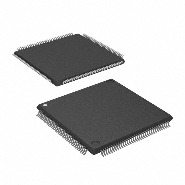
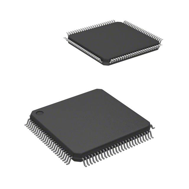
| Package / Case | 144-LQFP | |
| Product Status | Obsolete | |
| Supplier Device Package | 144-TQFP (20x20) | |
| Programmable | Not Verified | |
| Number of Logic Elements/Cells | 1500 | |
| Total RAM Bits | 18432 | |
| Number of I/O | 97 |
Blog


 Unveiling the Future: The Surge of Microcontrollers in 2024In the dynamic world of electronic components, microcontrollers stand out as a testament to innovation and versatility. As we edge closer to 2024, the landscape for microcontrollers and semiconductors, spearheaded by giants like STMicroelectronics, Texas Instruments, and Microchip, is set for remarkable transformation.
 Microcontrollers vs. Microprocessors: Unveiling the Core Differences for Embedded Systems EngineeringSeasoned professionals in the realm of embedded systems engineering and product development within the electronics sphere often grapple with distinguishing between microcontrollers and microprocessors. Despite their foundational role in the design and fabrication of a myriad of electronic gadgets, understanding their unique functionalities based on mere definitions can be challenging:
 A Deep Dive into the Global Ceramic Capacitors MarketJoin us in exploring the emerging subplot of environmental consciousness within the global ceramic capacitors market.
 Mastering Current Measurement with MicrocontrollersUnlock precise current measurement secrets with Microcontrollers! Conquer challenges, meet superhero solutions, and revolutionize accuracy with on-chip Analog Core Independent Peripherals (CIPs).
 What is a Rectifier Diode: A Guide to BeginnersMeet the unsung heroes of electronics—Rectifier Diodes! Explore their magic, applications, and join the behind-the-scenes adventure into gadget power.


$2.77
Price update:a months ago
Available in stock:
2035
Lattice Semiconductor Corporation
Lattice Semiconductor leads in low-power programmability, solving complex challenges across networks, from Edge to Cloud. With a foothold in communication, computing, industry, autos, and consumers, they nurture lasting relationships, offering world-class support for unfettered innovation, crafting a secure, connected world.
View All Product from Lattice Semiconductor CorporationBlog
- Unveiling the Future: The Surge of Microcontrollers in 2024In the dynamic world of electronic components, microcontrollers stand out as a testament to innovation and versatility. As we edge closer to 2024, the landscape for microcontrollers and semiconductors, spearheaded by giants like STMicroelectronics, Texas Instruments, and Microchip, is set for remarkable transformation.
- Microcontrollers vs. Microprocessors: Unveiling the Core Differences for Embedded Systems EngineeringSeasoned professionals in the realm of embedded systems engineering and product development within the electronics sphere often grapple with distinguishing between microcontrollers and microprocessors. Despite their foundational role in the design and fabrication of a myriad of electronic gadgets, understanding their unique functionalities based on mere definitions can be challenging:
- A Deep Dive into the Global Ceramic Capacitors MarketJoin us in exploring the emerging subplot of environmental consciousness within the global ceramic capacitors market.
- Mastering Current Measurement with MicrocontrollersUnlock precise current measurement secrets with Microcontrollers! Conquer challenges, meet superhero solutions, and revolutionize accuracy with on-chip Analog Core Independent Peripherals (CIPs).
- What is a Rectifier Diode: A Guide to BeginnersMeet the unsung heroes of electronics—Rectifier Diodes! Explore their magic, applications, and join the behind-the-scenes adventure into gadget power.
Popular Manufacturers
View all manufactures More


Popular Parts Number
More Electronic Parts More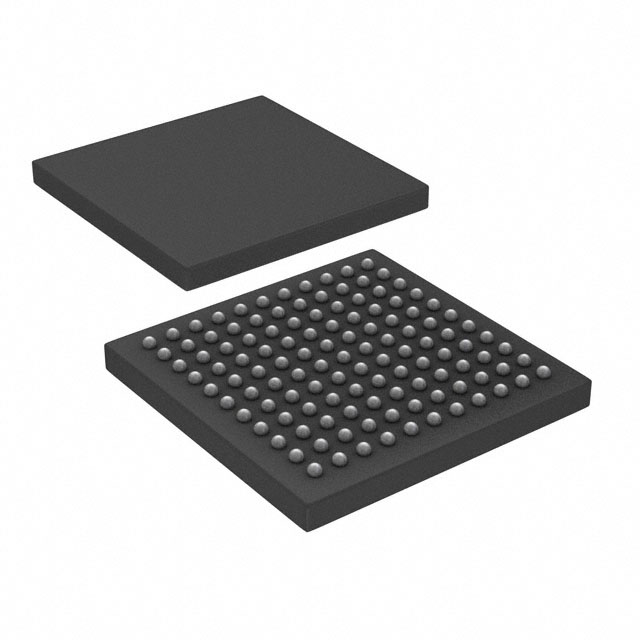
ICE40HX4K-BG121
IC FPGA 93 I/O 121CABGA
LCMXO2-7000HC-6TG144C
IC FPGA 114 I/O 144TQFP
LCMXO3LF-1300E-5UWG36ITR1K
IC FPGA 28 I/O 36WLCSP
ICE40LP1K-CM81
IC FPGA 63 I/O 81UCBGA

ICE5LP4K-SWG36ITR1K
IC FPGA 26 I/O 36WLCSP
LCMXO256C-5TN100C
IC FPGA 78 I/O 100TQFP
LCMXO2-1200UHC-4FTG256I
IC FPGA 206 I/O 256FTBGA
LFE5U-25F-8BG381C
IC FPGA 197 I/O 381CABGA
LCMXO1200C-4TN100C
IC FPGA 73 I/O 100TQFP
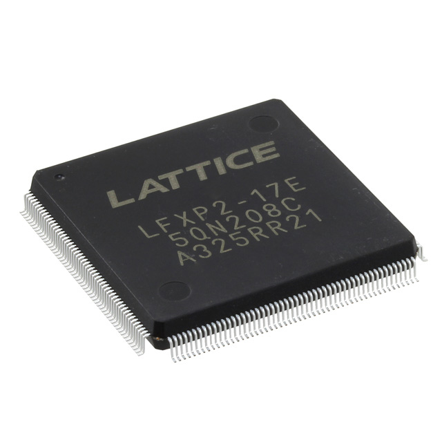
LFXP2-5E-5QN208C
IC FPGA 146 I/O 208QFP