


$124.47
Price update:a months ago
Available in stock:
800


45
Serves customers in 45 countries
1000+
Worldwide Manufacturers
$140M
$140M Growth in 5 Years
50.0M+
50M Parts Shipped in 5 Years

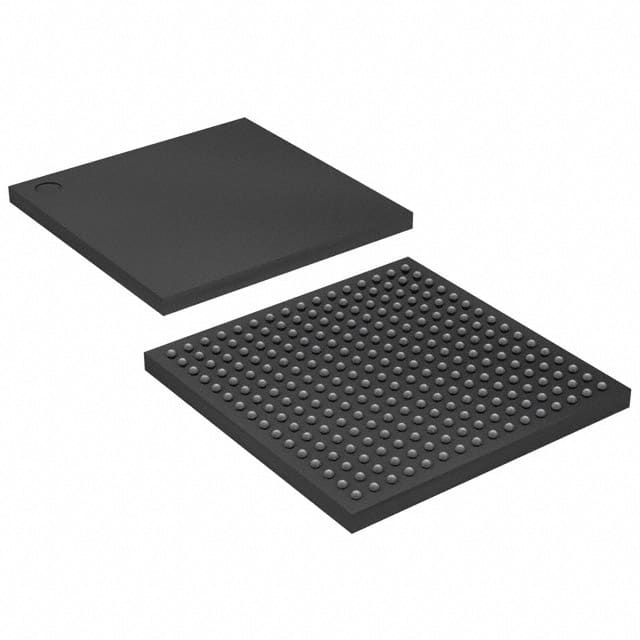
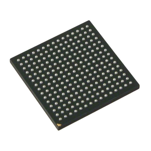
Xilinx
Xilinx stands as a preeminent purveyor of All Programmable Field-Programmable Gate Arrays (FPGAs), System on Chips (SoCs), Multiprocessor System on Chips (MPSoCs), and Three-Dimensional Integrated Circuits (3D ICs). AMD stands in a distinctive position, facilitating applications that embody a dual nature of software-defined sophistication and hardware-honed optimization. This empowering of industries finds its zenith in the realms of Cloud Computing, 5G Wireless Connectivity, Embedded Vision, and the sprawling domain of Industrial Internet of Things (IIoT).
View All Product from Xilinx


Features
• Fast, high-density Field Programmable Gate Arrays
- Densities from 50k to 1M system gates
- System performance up to 200 MHz
- 66-MHz PCI Compliant
- Hot-swappable for Compact PCI
• Multi-standard SelectIO™ interfaces
- 16 high-performance interface standards
- Connects directly to ZBTRAM devices
• Built-in clock-management circuitry
- Four dedicated delay-locked loops (DLLs) for advanced clock control
- Four primary low-skew global clock distribution nets, plus 24 secondary local clock nets
• Hierarchical memory system
- LUTs configurable as 16-bit RAM, 32-bit RAM, 16-bit dual-ported RAM, or 16-bit Shift Register
- Configurable synchronous dual-ported 4k-bit RAMs
- Fast interfaces to external high-performance RAMs
• Flexible architecture that balances speed and density
- Dedicated carry logic for high-speed arithmetic
- Dedicated multiplier support
- Cascade chain for wide-input functions
- Abundant registers/latches with clock enable, and dual synchronous/asynchronous set and reset
- Internal 3-state bussing
- IEEE 1149.1 boundary-scan logic
- Die-temperature sensor diode
• Supported by FPGA Foundation™ and Alliance Development Systems
- Complete support for Unified Libraries, Relationally Placed Macros, and Design Manager
- Wide selection of PC and workstation platforms
• SRAM-based in-system configuration
- Unlimited re-programmability
- Four programming modes
• 0.22 μm 5-layer metal process
• 100% factory tested
Description
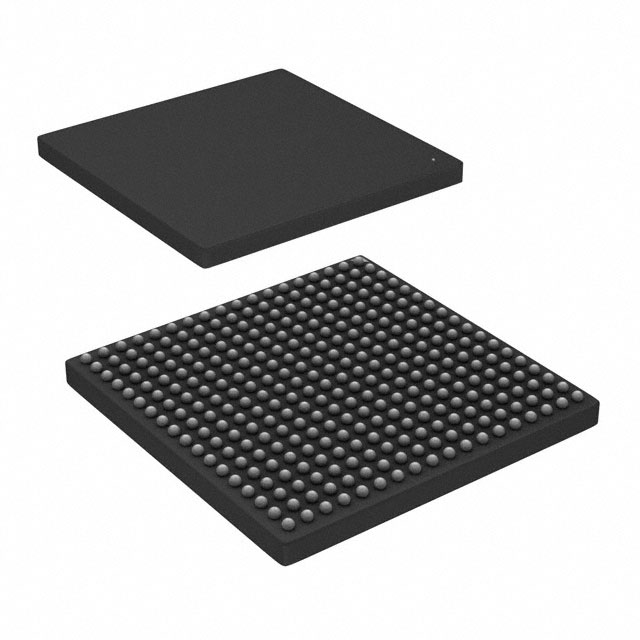
The Virtex FPGA family delivers high-performance, high-capacity programmable logic solutions. Dramatic increases in silicon efficiency result from optimizing the new architecture for place-and-route efficiency and exploiting an aggressive 5-layer-metal 0.22 μm CMOS process. These advances make Virtex FPGAs powerful and flexible alternatives to mask-programmed gate arrays. The Virtex family comprises the nine members shown in Table 1.
Building on experience gained from previous generations of FPGAs, the Virtex family represents a revolutionary step forward in programmable logic design. Combining a wide variety of programmable system features, a rich hierarchy of fast, flexible interconnect resources, and advanced process technology, the Virtex family delivers a high-speed and high-capacity programmable logic solution that enhances design flexibility while reducing time-to-market.
Feature
• Fast, high-density Field Programmable Gate Arrays
- Densities from 50k to 1M system gates
- System performance up to 200 MHz
- 66-MHz PCI Compliant
- Hot-swappable for Compact PCI
• Multi-standard SelectIO™ interfaces
- 16 high-performance interface standards
- Connects directly to ZBTRAM devices
• Built-in clock-management circuitry
- Four dedicated delay-locked loops (DLLs) for advanced clock control
- Four primary low-skew global clock distribution nets, plus 24 secondary local clock nets
• Hierarchical memory system
- LUTs configurable as 16-bit RAM, 32-bit RAM, 16-bit dual-ported RAM, or 16-bit Shift Register
- Configurable synchronous dual-ported 4k-bit RAMs
- Fast interfaces to external high-performance RAMs
• Flexible architecture that balances speed and density
- Dedicated carry logic for high-speed arithmetic
- Dedicated multiplier support
- Cascade chain for wide-input functions
- Abundant registers/latches with clock enable, and dual synchronous/asynchronous set and reset
- Internal 3-state bussing
- IEEE 1149.1 boundary-scan logic
- Die-temperature sensor diode
• Supported by FPGA Foundation™ and Alliance
Development Systems
- Complete support for Unified Libraries, Relationally
Placed Macros, and Design Manager
- Wide selection of PC and workstation platforms
• SRAM-based in-system configuration
- Unlimited re-programmability
- Four programming modes
• 0.22 μm 5-layer metal process
• 100% factory tested


Related Products
| Mfr Part # | Price ($) | Quantity Available | |
|---|---|---|---|
 XCV200E-8PQ240CIC FPGA 158 I/O 240QFP | 27.66 |
191
Marketplace | |
XCV300-4BG432IIC FPGA 316 I/O 432MBGA | 3.46 |
348
Marketplace | |
 XCV300-4FG456CIC FPGA 312 I/O 456FBGA | 207.45 |
313
Marketplace | |
XCV300-4FG456IIC FPGA 312 I/O 456FBGA | 94.74 |
556
Marketplace | |
XCV300-4BG352IIC FPGA 260 I/O 352MBGA | 62.24 |
145
Marketplace | |
XCV300-4BG432CIC FPGA 316 I/O 432MBGA | 89.90 |
800
Marketplace |
Product Attributes
| TYPE | DESCRIPTION | Select all |
|---|---|---|
| Number of Gates | 322970 | |
| Voltage - Supply | 2.375V ~ 2.625V | |
| Mounting Type | Surface Mount | |
| Series | Virtex® | |
| Operating Temperature | 0°C ~ 85°C (TJ) | |
| Package | Tray | |
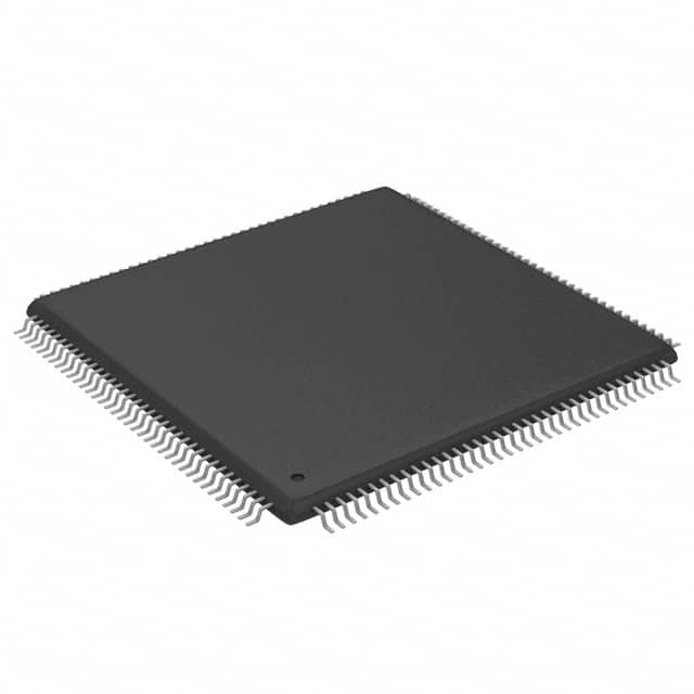
| Package / Case | 240-BFQFP | |
| Product Status | Obsolete | |
| Supplier Device Package | 240-PQFP (32x32) | |
| Programmable | Not Verified | |
| Number of LABs/CLBs | 1536 | |
| Number of Logic Elements/Cells | 6912 | |
| Total RAM Bits | 65536 | |
| Number of I/O | 166 |
Blog


 Unveiling the Future: The Surge of Microcontrollers in 2024In the dynamic world of electronic components, microcontrollers stand out as a testament to innovation and versatility. As we edge closer to 2024, the landscape for microcontrollers and semiconductors, spearheaded by giants like STMicroelectronics, Texas Instruments, and Microchip, is set for remarkable transformation.
 Microcontrollers vs. Microprocessors: Unveiling the Core Differences for Embedded Systems EngineeringSeasoned professionals in the realm of embedded systems engineering and product development within the electronics sphere often grapple with distinguishing between microcontrollers and microprocessors. Despite their foundational role in the design and fabrication of a myriad of electronic gadgets, understanding their unique functionalities based on mere definitions can be challenging:
 A Deep Dive into the Global Ceramic Capacitors MarketJoin us in exploring the emerging subplot of environmental consciousness within the global ceramic capacitors market.
 Mastering Current Measurement with MicrocontrollersUnlock precise current measurement secrets with Microcontrollers! Conquer challenges, meet superhero solutions, and revolutionize accuracy with on-chip Analog Core Independent Peripherals (CIPs).
 What is a Rectifier Diode: A Guide to BeginnersMeet the unsung heroes of electronics—Rectifier Diodes! Explore their magic, applications, and join the behind-the-scenes adventure into gadget power.


$124.47
Price update:a months ago
Available in stock:
800
Xilinx
Xilinx stands as a preeminent purveyor of All Programmable Field-Programmable Gate Arrays (FPGAs), System on Chips (SoCs), Multiprocessor System on Chips (MPSoCs), and Three-Dimensional Integrated Circuits (3D ICs). AMD stands in a distinctive position, facilitating applications that embody a dual nature of software-defined sophistication and hardware-honed optimization. This empowering of industries finds its zenith in the realms of Cloud Computing, 5G Wireless Connectivity, Embedded Vision, and the sprawling domain of Industrial Internet of Things (IIoT).
View All Product from XilinxBlog
- Unveiling the Future: The Surge of Microcontrollers in 2024In the dynamic world of electronic components, microcontrollers stand out as a testament to innovation and versatility. As we edge closer to 2024, the landscape for microcontrollers and semiconductors, spearheaded by giants like STMicroelectronics, Texas Instruments, and Microchip, is set for remarkable transformation.
- Microcontrollers vs. Microprocessors: Unveiling the Core Differences for Embedded Systems EngineeringSeasoned professionals in the realm of embedded systems engineering and product development within the electronics sphere often grapple with distinguishing between microcontrollers and microprocessors. Despite their foundational role in the design and fabrication of a myriad of electronic gadgets, understanding their unique functionalities based on mere definitions can be challenging:
- A Deep Dive into the Global Ceramic Capacitors MarketJoin us in exploring the emerging subplot of environmental consciousness within the global ceramic capacitors market.
- Mastering Current Measurement with MicrocontrollersUnlock precise current measurement secrets with Microcontrollers! Conquer challenges, meet superhero solutions, and revolutionize accuracy with on-chip Analog Core Independent Peripherals (CIPs).
- What is a Rectifier Diode: A Guide to BeginnersMeet the unsung heroes of electronics—Rectifier Diodes! Explore their magic, applications, and join the behind-the-scenes adventure into gadget power.
Popular Manufacturers
View all manufactures More


Popular Parts Number
More Electronic Parts More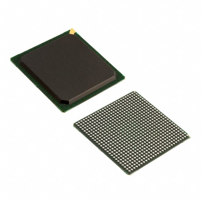
XC6SLX75-N3FGG676C
IC FPGA 408 I/O 676FBGA
XC2S30-5TQG144C
IC FPGA 92 I/O 144TQFP

XC7S50-2CSGA324C
IC FPGA 210 I/O 324CSBGA

XC7A50T-2FTG256I
IC FPGA 170 I/O 256FTBGA
XC6SLX25-2CSG324I
IC FPGA 226 I/O 324CSBGA
XC7A50T-2CSG325I
IC FPGA 150 I/O 324CSBGA
XC7A75T-2FTG256I
IC FPGA 170 I/O 256FTBGA
XC7A200T-1FFG1156I
IC FPGA 500 I/O 1156FCBGA
XC7K160T-2FBG484I
IC FPGA 285 I/O 484FCBGA
XC7S15-2CSGA225I
IC FPGA 100 I/O 225CSBGA