


$110.24
Price update:a months ago
Available in stock:
2000


45
Serves customers in 45 countries
1000+
Worldwide Manufacturers
$140M
$140M Growth in 5 Years
50.0M+
50M Parts Shipped in 5 Years

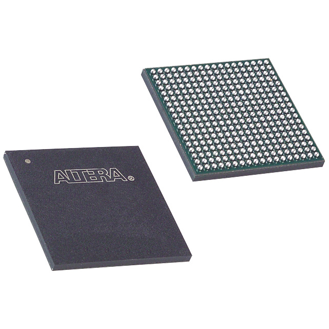
Altera
On June 1, 2015, Intel and Altera unveiled a transformative accord. Intel's acquisition of Altera concluded on December 28, 2015. This amalgamation melded Intel's cutting-edge products and manufacturing prowess with Altera's pioneering field-programmable gate array (FPGA) technology. The synergy birthed novel product classes, catering adeptly to data centers and the burgeoning Internet of Things (IoT) domain.
View All Product from Altera


Features
■ Programmable logic devices (PLDs), providing low cost system-on-a-programmable-chip (SOPC) integration in a single device
– Enhanced embedded array for implementing megafunctions such as efficient memory and specialized logic functions
– Dual-port capability with up to 16-bit width per embedded array block (EAB)
– Logic array for general logic functions
■ High density
– 10,000 to 100,000 typical gates (see Table 1)
– Up to 49,152 RAM bits (4,096 bits per EAB, all of which can be used without reducing logic capacity)
■ Cost-efficient programmable architecture for high-volume applications
– Cost-optimized process
– Low cost solution for high-performance communications applications
■ System-level features
– MultiVoltTM I/O pins can drive or be driven by 2.5-V, 3.3-V, or 5.0-V devices
– Low power consumption
– Bidirectional I/O performance (setup time [tSU] and clock-tooutput delay [tCO]) up to 250 MHz
– Fully compliant with the peripheral component interconnect Special Interest Group (PCI SIG) PCI Local Bus Specification, Revision 2.2 for 3.3-V operation at 33 MHz or 66 MHz
■ Extended temperature range
More Features
– -1 speed grade devices are compliant with PCI Local Bus Specification, Revision 2.2 for 5.0-V operation
– Built-in Joint Test Action Group (JTAG) boundary-scan test (BST) circuitry compliant with IEEE Std. 1149.1-1990, available without consuming additional device logic.
– Operate with a 2.5-V internal supply voltage
– In-circuit reconfigurability (ICR) via external configuration devices, intelligent controller, or JTAG port
– ClockLockTM and ClockBoostTM options for reduced clock delay, clock skew, and clock multiplication
– Built-in, low-skew clock distribution trees
– 100% functional testing of all devices; test vectors or scan chains are not required
– Pull-up on I/O pins before and during configuration
■ Flexible interconnect
– FastTrack® Interconnect continuous routing structure for fast, predictable interconnect delays
– Dedicated carry chain that implements arithmetic functions such as fast adders, counters, and comparators (automatically used by software tools and megafunctions)
– Dedicated cascade chain that implements high-speed, high-fan-in logic functions (automatically used by software tools and megafunctions)
– Tri-state emulation that implements internal tri-state buses
– Up to six global clock signals and four global clear signals
■ Powerful I/O pins
– Individual tri-state output enable control for each pin
– Open-drain option on each I/O pin
– Programmable output slew-rate control to reduce switching noise
– Clamp to VCCIO user-selectable on a pin-by-pin basis
– Supports hot-socketing
■ Software design support and automatic place-and-route provided by Altera development systems for Windows-based PCs and Sun SPARCstation, and HP 9000 Series 700/800 workstations
■ Flexible package options are available in 100 to 484 pins, including the innovative FineLine BGATM packages (see Tables 2 and 3)
■ Additional design entry and simulation support provided by EDIF 2 0 0 and 3 0 0 netlist files, library of parameterized modules (LPM), DesignWare components, Verilog HDL, VHDL, and other interfaces to popular EDA tools from manufacturers such as Cadence, Exemplar Logic, Mentor Graphics, OrCAD, Synopsys, Synplicity, VeriBest, and Viewlogic
Feature
■ Programmable logic devices (PLDs), providing low cost system-on-a-programmable-chip (SOPC) integration in a single device
– Enhanced embedded array for implementing megafunctions such as efficient memory and specialized logic functions
– Dual-port capability with up to 16-bit width per embedded array block (EAB)
– Logic array for general logic functions
■ High density
– 10,000 to 100,000 typical gates (see Table 1)
– Up to 49,152 RAM bits (4,096 bits per EAB, all of which can be used without reducing logic capacity)
■ Cost-efficient programmable architecture for high-volume applications
– Cost-optimized process
– Low cost solution for high-performance communications applications


Related Products
| Mfr Part # | Price ($) | Quantity Available | |
|---|---|---|---|
 EP1K30TC144-3NIC FPGA 102 I/O 144TQFP | 15.16 |
2265
Marketplace | |
EP1K30TI144-2NIC FPGA 102 I/O 144TQFP | 75.79 |
720
Marketplace |
Product Attributes
| TYPE | DESCRIPTION | Select all |
|---|---|---|
| Number of Gates | 199000 | |
| Voltage - Supply | 2.375V ~ 2.625V | |
| Mounting Type | Surface Mount | |
| Series | ACEX-1K® | |
| Operating Temperature | 0°C ~ 70°C (TA) | |
| Package | Tray | |
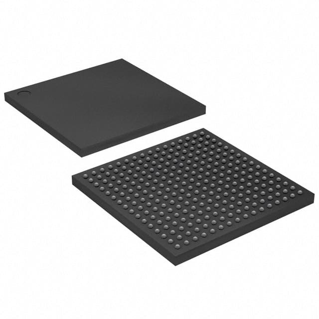
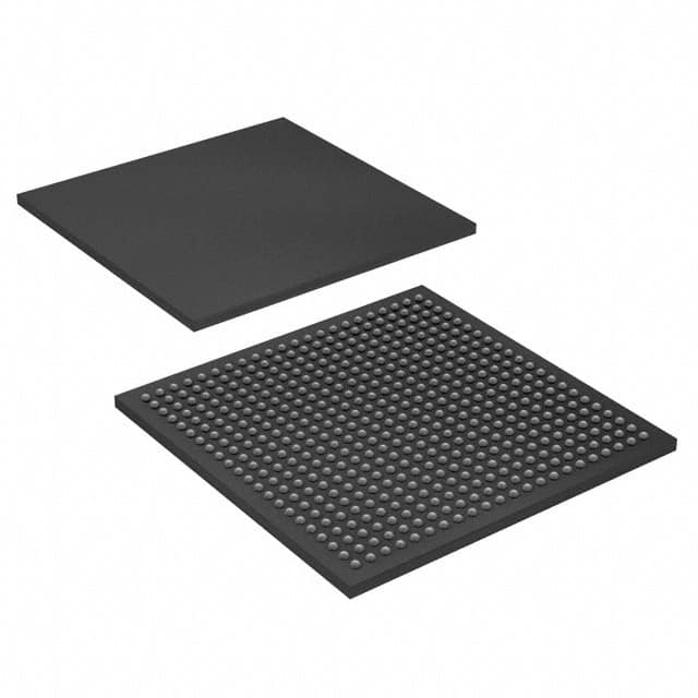
| Package / Case | 256-BGA | |
| Product Status | Obsolete | |
| Supplier Device Package | 256-FBGA (17x17) | |
| Programmable | Not Verified | |
| Number of LABs/CLBs | 360 | |
| Number of Logic Elements/Cells | 2880 | |
| Total RAM Bits | 40960 | |
| Number of I/O | 186 |
Blog


 Unveiling the Future: The Surge of Microcontrollers in 2024In the dynamic world of electronic components, microcontrollers stand out as a testament to innovation and versatility. As we edge closer to 2024, the landscape for microcontrollers and semiconductors, spearheaded by giants like STMicroelectronics, Texas Instruments, and Microchip, is set for remarkable transformation.
 Microcontrollers vs. Microprocessors: Unveiling the Core Differences for Embedded Systems EngineeringSeasoned professionals in the realm of embedded systems engineering and product development within the electronics sphere often grapple with distinguishing between microcontrollers and microprocessors. Despite their foundational role in the design and fabrication of a myriad of electronic gadgets, understanding their unique functionalities based on mere definitions can be challenging:
 A Deep Dive into the Global Ceramic Capacitors MarketJoin us in exploring the emerging subplot of environmental consciousness within the global ceramic capacitors market.
 Mastering Current Measurement with MicrocontrollersUnlock precise current measurement secrets with Microcontrollers! Conquer challenges, meet superhero solutions, and revolutionize accuracy with on-chip Analog Core Independent Peripherals (CIPs).
 What is a Rectifier Diode: A Guide to BeginnersMeet the unsung heroes of electronics—Rectifier Diodes! Explore their magic, applications, and join the behind-the-scenes adventure into gadget power.


$110.24
Price update:a months ago
Available in stock:
2000
Altera
On June 1, 2015, Intel and Altera unveiled a transformative accord. Intel's acquisition of Altera concluded on December 28, 2015. This amalgamation melded Intel's cutting-edge products and manufacturing prowess with Altera's pioneering field-programmable gate array (FPGA) technology. The synergy birthed novel product classes, catering adeptly to data centers and the burgeoning Internet of Things (IoT) domain.
View All Product from AlteraBlog
- Unveiling the Future: The Surge of Microcontrollers in 2024In the dynamic world of electronic components, microcontrollers stand out as a testament to innovation and versatility. As we edge closer to 2024, the landscape for microcontrollers and semiconductors, spearheaded by giants like STMicroelectronics, Texas Instruments, and Microchip, is set for remarkable transformation.
- Microcontrollers vs. Microprocessors: Unveiling the Core Differences for Embedded Systems EngineeringSeasoned professionals in the realm of embedded systems engineering and product development within the electronics sphere often grapple with distinguishing between microcontrollers and microprocessors. Despite their foundational role in the design and fabrication of a myriad of electronic gadgets, understanding their unique functionalities based on mere definitions can be challenging:
- A Deep Dive into the Global Ceramic Capacitors MarketJoin us in exploring the emerging subplot of environmental consciousness within the global ceramic capacitors market.
- Mastering Current Measurement with MicrocontrollersUnlock precise current measurement secrets with Microcontrollers! Conquer challenges, meet superhero solutions, and revolutionize accuracy with on-chip Analog Core Independent Peripherals (CIPs).
- What is a Rectifier Diode: A Guide to BeginnersMeet the unsung heroes of electronics—Rectifier Diodes! Explore their magic, applications, and join the behind-the-scenes adventure into gadget power.
Popular Manufacturers
View all manufactures More


Popular Parts Number
More Electronic Parts More
EP4CE6U14I7N
IC FPGA 179 I/O 256UBGA
5CGXFC3B7U15C8N
IC FPGA 144 I/O 324UBGA
EP4CGX30CF19C7N
IC FPGA 150 I/O 324FBGA

EP4CE40F23C6N
IC FPGA 328 I/O 484FBGA
5CGXFC7C6F23C7N
IC FPGA 240 I/O 484FBGA
EP4CE6F17C8
IC FPGA 179 I/O 256FBGA
EP3C5E144C8
IC FPGA 94 I/O 144EQFP
EP2C5AF256I8N
IC FPGA 158 I/O 256FBGA
EP2C15AF484C6NES
IC FPGA 315 I/O 484FBGA
EP4CE30F23C8LN
IC FPGA 328 I/O 484FBGA