
XC2C512-10FGG324I
Compare
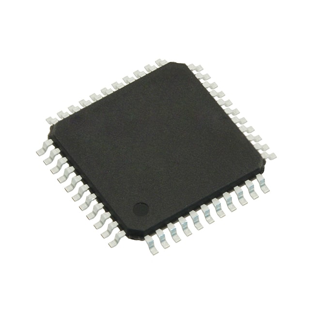
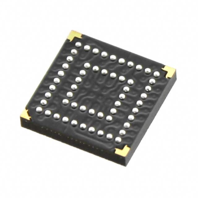
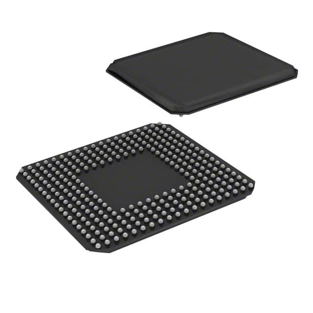
XC2C512-10FGG324I
IC CPLD 512MC 9.2NS 324FBGA


Compare
$89.90
Price update:a months ago
Available in stock:
500


45
Serves customers in 45 countries
1000+
Worldwide Manufacturers
$140M
$140M Growth in 5 Years
50.0M+
50M Parts Shipped in 5 Years

AMD
AMD stands as a preeminent purveyor of All Programmable Field-Programmable Gate Arrays (FPGAs), System-on-Chips (SoCs), Multiprocessor SoCs (MPSoCs), and Three-Dimensional Integrated Circuits (3D ICs). Notably, AMD confers singular prowess in facilitating software-defined and hardware-optimized applications, thus propelling progress across domains like Cloud Computing, 5G Wireless, Embedded Vision, and Industrial Internet of Things (IoT).
View All Product from AMD


The CoolRunner-II 512-macrocell device is designed for both high performance and low power applications. This lends power savings to high-end communication equipment and high speed to battery operated devices. Due to the low power stand-by and dynamic operation, overall system reliability is improved This device consists of thirty two Function Blocks inter-connected by a low power Advanced Interconnect Matrix (AIM). The AIM feeds 40 true and complement inputs to each Function Block. The Function Blocks consist of a 40 by 56 P-term PLA and 16 macrocells which contain numerous configuration bits that allow for combinational or registered modes of operation. Additionally, these registers can be globally reset or preset and configured as a D or T flip-flop or as a D latch. There are also multiple clock signals, both global and local product term types, configured on a per macrocell basis. Output pin configurations include slew rate limit, bus hold, pull-up, open drain and programmable grounds.
A Schmitt-trigger input is available on a per input pin basis. In addition to storing macrocell output states, the macrocell registers may be configured as "direct input" registers to store signals directly from input pins. Clocking is available on a global or Function Block basis. Three global clocks are available for all Function Blocks as a synchronous clock source. Macrocell registers can be individually configured to power up to the zero or one state. A global set/reset control line is also available to asynchronously set or reset selected registers during operation. Additional local clock, synchronous clock-enable, asynchronous set/reset and output enable signals can be formed using product terms on a per-macrocell or per-Function Block basis. A DualEDGE flip-flop feature is also available on a per macrocell basis. This feature allows high performance synchronous operation based on lower frequency clocking to help reduce the total power consumption of the device. Circuitry has also been included to divide one externally supplied global clock (GCK2) by eight different selections. This yields divide by even and odd clock frequencies.
Feature
• Optimized for 1.8V systems
- As fast as 7.1 ns pin-to-pin delays
- As low as 14 μA quiescent current
• Industry’s best 0.18 micron CMOS CPLD
- Optimized architecture for effective logic synthesis
- Multi-voltage I/O operation — 1.5V to 3.3V
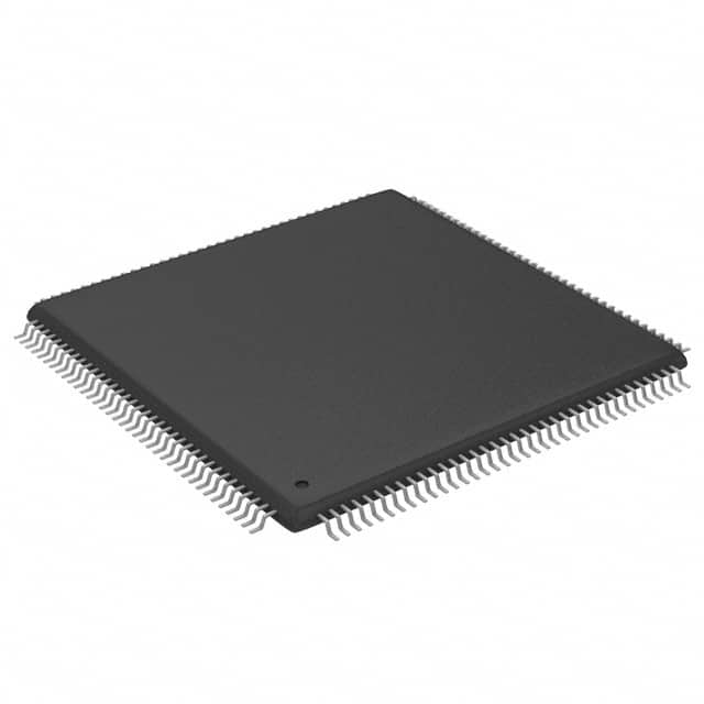
• Available in multiple package options
- 208-pin PQFP with 173 user I/O
- 256-ball FT (1.0mm) BGA with 212 user I/O
- 324-ball FG (1.0mm) BGA with 270 user I/O
- Pb-free available for all packages
• Advanced system features
- Fastest in system programming
· 1.8V ISP using IEEE 1532 (JTAG) interface
- IEEE1149.1 JTAG Boundary Scan Test
- Optional Schmitt-trigger input (per pin)
- Unsurpassed low power management
· DataGATE enable signal control
- Four separate I/O banks
- RealDigital 100% CMOS product term generation
- Flexible clocking modes
· Optional DualEDGE triggered registers
· Clock divider (divide by 2,4,6,8,10,12,14,16)
· CoolCLOCK
- Global signal options with macrocell control
· Multiple global clocks with phase selection per
macrocell
· Multiple global output enables
· Global set/reset
- Advanced design security
- PLA architecture
· Superior pinout retention
· 100% product term routability across function block
- Open-drain output option for Wired-OR and LED drive
- Optional bus-hold, 3-state or weak pullup on selected I/O pins
- Optional configurable grounds on unused I/Os
- Mixed I/O voltages compatible with 1.5V, 1.8V, 2.5V, and 3.3V logic levels
· SSTL2-1, SSTL3-1, and HSTL-1 I/O compatibility
- Hot Pluggable


Related Products
| Mfr Part # | Price ($) | Quantity Available | |
|---|---|---|---|
 XC2C384-7TQ144CIC CPLD 384MC 7.1NS 100TQFP | 16.60 |
2213
Marketplace | |
 XC2C384-7FTG256CIC CPLD 384MC 7.1NS 256FTBGA | 62.24 |
1128
Marketplace | |
 XC2C384-7FT256CIC CPLD 384MC 7.1NS 256FTBGA | 13.83 |
276
Marketplace | |
 XC2C512-10FG324IIC CPLD 512MC 9.2NS 324FBGA | 55.32 |
450
Marketplace | |
 XC2C384-10TQ144IIC CPLD 384MC 9.2NS 100TQFP | 221.28 |
250
Marketplace | |
 XC2C384-7PQ208CIC CPLD 384MC 7.1NS 208QFP | 20.75 |
3683
Marketplace |
Product Attributes
| TYPE | DESCRIPTION | Select all |
|---|---|---|
| Package / Case | 324-BBGA | |
| Programmable | Not Verified | |
| Supplier Device Package | 324-FBGA (23x23) | |
| Programmable Type | In System Programmable | |
| Delay Time tpd(1) Max | 9.2 ns | |
| Voltage Supply - Internal | 1.7V ~ 1.9V | |
| Number of Logic Elements/Blocks | 32 | |
| Number of Macrocells | 512 | |
| Number of Gates | 12000 | |
| Number of I/O | 270 | |
| Series | CoolRunner II | |
| Operating Temperature | -40°C ~ 85°C (TA) | |
| Package | Tray | |
| Mounting Type | Surface Mount | |
| Product Status | Active |
Blog


 Unveiling the Future: The Surge of Microcontrollers in 2024In the dynamic world of electronic components, microcontrollers stand out as a testament to innovation and versatility. As we edge closer to 2024, the landscape for microcontrollers and semiconductors, spearheaded by giants like STMicroelectronics, Texas Instruments, and Microchip, is set for remarkable transformation.
 Microcontrollers vs. Microprocessors: Unveiling the Core Differences for Embedded Systems EngineeringSeasoned professionals in the realm of embedded systems engineering and product development within the electronics sphere often grapple with distinguishing between microcontrollers and microprocessors. Despite their foundational role in the design and fabrication of a myriad of electronic gadgets, understanding their unique functionalities based on mere definitions can be challenging:
 A Deep Dive into the Global Ceramic Capacitors MarketJoin us in exploring the emerging subplot of environmental consciousness within the global ceramic capacitors market.
 Mastering Current Measurement with MicrocontrollersUnlock precise current measurement secrets with Microcontrollers! Conquer challenges, meet superhero solutions, and revolutionize accuracy with on-chip Analog Core Independent Peripherals (CIPs).
 What is a Rectifier Diode: A Guide to BeginnersMeet the unsung heroes of electronics—Rectifier Diodes! Explore their magic, applications, and join the behind-the-scenes adventure into gadget power.


$89.90
Price update:a months ago
Available in stock:
500
AMD
AMD stands as a preeminent purveyor of All Programmable Field-Programmable Gate Arrays (FPGAs), System-on-Chips (SoCs), Multiprocessor SoCs (MPSoCs), and Three-Dimensional Integrated Circuits (3D ICs). Notably, AMD confers singular prowess in facilitating software-defined and hardware-optimized applications, thus propelling progress across domains like Cloud Computing, 5G Wireless, Embedded Vision, and Industrial Internet of Things (IoT).
View All Product from AMDBlog
- Unveiling the Future: The Surge of Microcontrollers in 2024In the dynamic world of electronic components, microcontrollers stand out as a testament to innovation and versatility. As we edge closer to 2024, the landscape for microcontrollers and semiconductors, spearheaded by giants like STMicroelectronics, Texas Instruments, and Microchip, is set for remarkable transformation.
- Microcontrollers vs. Microprocessors: Unveiling the Core Differences for Embedded Systems EngineeringSeasoned professionals in the realm of embedded systems engineering and product development within the electronics sphere often grapple with distinguishing between microcontrollers and microprocessors. Despite their foundational role in the design and fabrication of a myriad of electronic gadgets, understanding their unique functionalities based on mere definitions can be challenging:
- A Deep Dive into the Global Ceramic Capacitors MarketJoin us in exploring the emerging subplot of environmental consciousness within the global ceramic capacitors market.
- Mastering Current Measurement with MicrocontrollersUnlock precise current measurement secrets with Microcontrollers! Conquer challenges, meet superhero solutions, and revolutionize accuracy with on-chip Analog Core Independent Peripherals (CIPs).
- What is a Rectifier Diode: A Guide to BeginnersMeet the unsung heroes of electronics—Rectifier Diodes! Explore their magic, applications, and join the behind-the-scenes adventure into gadget power.
Popular Manufacturers
View all manufactures More


Popular Parts Number
More Electronic Parts MoreXC2C512-10FGG324I
IC CPLD 512MC 9.2NS 324FBGA
XCR3032XL-10VQG44C
IC CPLD 32MC 9.1NS 44VQFP
XC9572XL-7TQG100C
IC CPLD 72MC 7.5NS 100TQFP

XC9536XL-10CS48C
IC CPLD 36MC 10NS 48CSBGA
XCR3032XL-10CSG48C
IC CPLD 32MC 9.1NS 48CSBGA
XC2C64A-7VQ100I
IC CPLD 64MC 6.7NS 100VQFP
XCR3064XL-10CPG56C
IC CPLD 64MC 9.1NS 56CSBGA

XC9572XL-5CS48C
IC CPLD 72MC 5NS 48CSBGA
XC95144XL-7TQG144I
IC CPLD 144MC 7.5NS 144TQFP
XC95288XL-7CSG280I
IC CPLD 288MC 7.5NS 280CSBGA