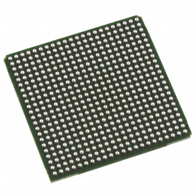
LFE3-70E-7FN484C
Compare
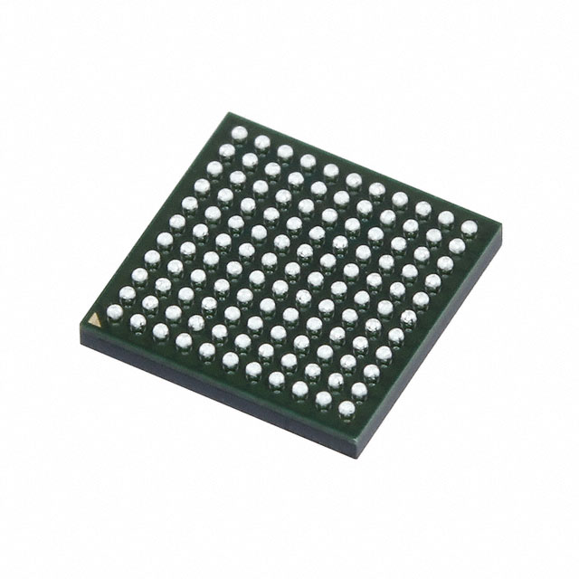
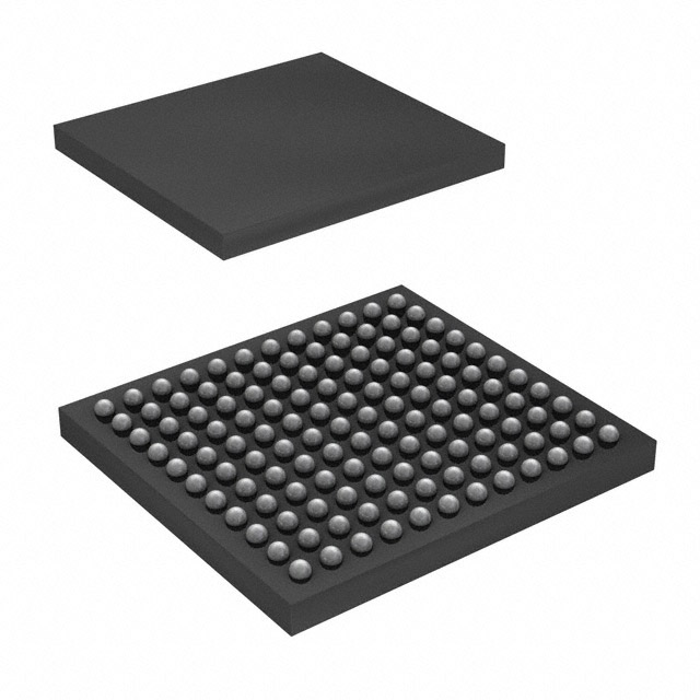
LFE3-70E-7FN484C
IC FPGA 295 I/O 484FBGA


Compare
Price negotiable
Price update:a months ago
Available in stock:
2580


45
Serves customers in 45 countries
1000+
Worldwide Manufacturers
$140M
$140M Growth in 5 Years
50.0M+
50M Parts Shipped in 5 Years

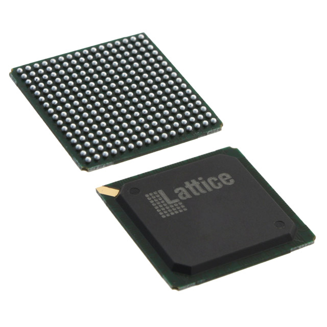
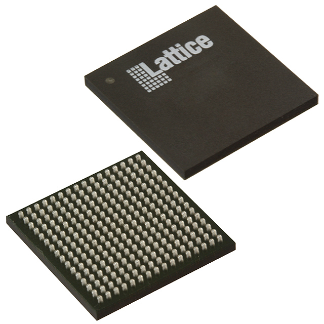
Lattice Semiconductor Corporation
Lattice Semiconductor leads in low-power programmability, solving complex challenges across networks, from Edge to Cloud. With a foothold in communication, computing, industry, autos, and consumers, they nurture lasting relationships, offering world-class support for unfettered innovation, crafting a secure, connected world.
View All Product from Lattice Semiconductor Corporation


The LatticeECP3™ (EConomy Plus Third generation) family of FPGA devices is optimized to deliver high performance features such as an enhanced DSP architecture, high speed SERDES and high speed source synchronous interfaces in an economical FPGA fabric. This combination is achieved through advances in device architecture and the use of 65 nm technology making the devices suitable for high-volume, high-speed, low-cost applications.
The LatticeECP3 device family expands look-up-table (LUT) capacity to 149K logic elements and supports up to 586 user I/Os. The LatticeECP3 device family also offers up to 320 18 x 18 multipliers and a wide range of parallel I/O standards.
The LatticeECP3 FPGA fabric is optimized with high performance and low cost in mind. The LatticeECP3 devices utilize reconfigurable SRAM logic technology and provide popular building blocks such as LUT-based logic, distributed and embedded memory, Phase Locked Loops (PLLs), Delay Locked Loops (DLLs), pre-engineered source synchronous I/O support, enhanced sysDSP slices and advanced configuration support, including encryption and dual-boot capabilities.
The pre-engineered source synchronous logic implemented in the LatticeECP3 device family supports a broad range of interface standards, including DDR3, XGMII and 7:1 LVDS.
The LatticeECP3 device family also features high speed SERDES with dedicated PCS functions. High jitter tolerance and low transmit jitter allow the SERDES plus PCS blocks to be configured to support an array of popular data protocols including PCI Express, SMPTE, Ethernet (XAUI, GbE, and SGMII) and CPRI. Transmit Pre-emphasis and Receive Equalization settings make the SERDES suitable for transmission and reception over various forms of media.
The LatticeECP3 devices also provide flexible, reliable and secure configuration options, such as dual-boot capability, bit-stream encryption, and TransFR field upgrade features.
The Lattice Diamond™ and ispLEVER® design software allows large complex designs to be efficiently implemented using the LatticeECP3 FPGA family. Synthesis library support for LatticeECP3 is available for popular logic synthesis tools. Diamond and ispLEVER tools use the synthesis tool output along with the constraints from its floor planning tools to place and route the design in the LatticeECP3 device. The tools extract the timing from the routing and back-annotate it into the design for timing verification.
Lattice provides many pre-engineered IP (Intellectual Property) modules for the LatticeECP3 family. By using these configurable soft core IPs as standardized blocks, designers are free to concentrate on the unique aspects of their design, increasing their productivity.
Feature
Higher Logic Density for Increased System Integration
• 17K to 149K LUTs
• 116 to 586 I/Os Embedded SERDES
• 150 Mbps to 3.2 Gbps for Generic 8b10b, 10-bit SERDES, and 8-bit SERDES modes
• Data Rates 230 Mbps to 3.2 Gbps per channel for all other protocols
• Up to 16 channels per device: PCI Express, SONET/SDH, Ethernet (1GbE, SGMII, XAUI), CPRI, SMPTE 3G and Serial RapidIO
sysDSP™
• Fully cascadable slice architecture
• 12 to 160 slices for high performance multiply and accumulate
• Powerful 54-bit ALU operations
• Time Division Multiplexing MAC Sharing
• Rounding and truncation
• Each slice supports
— Half 36x36, two 18x18 or four 9x9 multipliers
— Advanced 18x36 MAC and 18x18 MultiplyMultiply-Accumulate (MMAC) operations
Flexible Memory Resources
• Up to 6.85Mbits sysMEM™ Embedded Block RAM (EBR)
• 36K to 303K bits distributed RAM
sysCLOCK Analog PLLs and DLLs
• Two DLLs and up to ten PLLs per device
Pre-Engineered Source Synchronous I/O
• DDR registers in I/O cells
• Dedicated read/write levelling functionality
• Dedicated gearing logic
• Source synchronous standards support
— ADC/DAC, 7:1 LVDS, XGMII
— High Speed ADC/DAC devices
• Dedicated DDR/DDR2/DDR3 memory with DQS support
• Optional Inter-Symbol Interference (ISI) correction on outputs
Programmable sysI/O™ Buffer Supports Wide Range of Interfaces
• On-chip termination
• Optional equalization filter on inputs
• LVTTL and LVCMOS 33/25/18/15/12
• SSTL 33/25/18/15 I, II
• HSTL15 I and HSTL18 I, II
• PCI and Differential HSTL, SSTL
• LVDS, Bus-LVDS, LVPECL, RSDS, MLVDS
Flexible Device Configuration
• Dedicated bank for configuration I/Os
• SPI boot flash interface
• Dual-boot images supported
• Slave SPI
• TransFR™ I/O for simple field updates
• Soft Error Detect embedded macro
System Level Support
• IEEE 1149.1 and IEEE 1532 compliant
• Reveal Logic Analyzer
• ORCAstra FPGA configuration utility
• On-chip oscillator for initialization & general use
• 1.2 V core power supply


Related Products
| Mfr Part # | Price ($) | Quantity Available | |
|---|---|---|---|
 LFE3-35EA-8FN484CIC FPGA 295 I/O 484FBGA | 8.41 |
5626
Marketplace | |
 LFE3-17EA-7FTN256CIC FPGA 133 I/O 256FTBGA | 27.56 |
140
Marketplace | |
 LFE3-35EA-8FN484IIC FPGA 295 I/O 484FBGA | 117.13 |
800
Marketplace | |
 LFE3-35EA-8FTN256IIC FPGA 133 I/O 256FTBGA | 61.16 |
2766
Marketplace | |
 LFE3-17EA-6MG328CIC FPGA 116 I/O 328CSBGA | 28.94 |
670
Marketplace | |
LFE3-35EA-7FN484IIC FPGA 295 I/O 484FBGA | 110.24 |
3298
Marketplace |
Product Attributes
| TYPE | DESCRIPTION | Select all |
|---|---|---|
| Voltage - Supply | 1.14V ~ 1.26V | |
| Mounting Type | Surface Mount | |
| Series | ECP3 | |
| Operating Temperature | 0°C ~ 85°C (TJ) | |
| Package | Tray | |
| Package / Case | 484-BBGA | |
| Product Status | Obsolete | |
| Supplier Device Package | 484-FPBGA (23x23) | |
| Programmable | Not Verified | |
| Number of LABs/CLBs | 8375 | |
| Number of Logic Elements/Cells | 67000 | |
| Total RAM Bits | 4526080 | |
| Number of I/O | 295 |
Blog


 Unveiling the Future: The Surge of Microcontrollers in 2024In the dynamic world of electronic components, microcontrollers stand out as a testament to innovation and versatility. As we edge closer to 2024, the landscape for microcontrollers and semiconductors, spearheaded by giants like STMicroelectronics, Texas Instruments, and Microchip, is set for remarkable transformation.
 Microcontrollers vs. Microprocessors: Unveiling the Core Differences for Embedded Systems EngineeringSeasoned professionals in the realm of embedded systems engineering and product development within the electronics sphere often grapple with distinguishing between microcontrollers and microprocessors. Despite their foundational role in the design and fabrication of a myriad of electronic gadgets, understanding their unique functionalities based on mere definitions can be challenging:
 A Deep Dive into the Global Ceramic Capacitors MarketJoin us in exploring the emerging subplot of environmental consciousness within the global ceramic capacitors market.
 Mastering Current Measurement with MicrocontrollersUnlock precise current measurement secrets with Microcontrollers! Conquer challenges, meet superhero solutions, and revolutionize accuracy with on-chip Analog Core Independent Peripherals (CIPs).
 What is a Rectifier Diode: A Guide to BeginnersMeet the unsung heroes of electronics—Rectifier Diodes! Explore their magic, applications, and join the behind-the-scenes adventure into gadget power.


Price negotiable
Price update:a months ago
Available in stock:
2580
Lattice Semiconductor Corporation
Lattice Semiconductor leads in low-power programmability, solving complex challenges across networks, from Edge to Cloud. With a foothold in communication, computing, industry, autos, and consumers, they nurture lasting relationships, offering world-class support for unfettered innovation, crafting a secure, connected world.
View All Product from Lattice Semiconductor CorporationBlog
- Unveiling the Future: The Surge of Microcontrollers in 2024In the dynamic world of electronic components, microcontrollers stand out as a testament to innovation and versatility. As we edge closer to 2024, the landscape for microcontrollers and semiconductors, spearheaded by giants like STMicroelectronics, Texas Instruments, and Microchip, is set for remarkable transformation.
- Microcontrollers vs. Microprocessors: Unveiling the Core Differences for Embedded Systems EngineeringSeasoned professionals in the realm of embedded systems engineering and product development within the electronics sphere often grapple with distinguishing between microcontrollers and microprocessors. Despite their foundational role in the design and fabrication of a myriad of electronic gadgets, understanding their unique functionalities based on mere definitions can be challenging:
- A Deep Dive into the Global Ceramic Capacitors MarketJoin us in exploring the emerging subplot of environmental consciousness within the global ceramic capacitors market.
- Mastering Current Measurement with MicrocontrollersUnlock precise current measurement secrets with Microcontrollers! Conquer challenges, meet superhero solutions, and revolutionize accuracy with on-chip Analog Core Independent Peripherals (CIPs).
- What is a Rectifier Diode: A Guide to BeginnersMeet the unsung heroes of electronics—Rectifier Diodes! Explore their magic, applications, and join the behind-the-scenes adventure into gadget power.
Popular Manufacturers
View all manufactures More


Popular Parts Number
More Electronic Parts More
LCMXO1200C-4TN100C
IC FPGA 73 I/O 100TQFP
LFXP2-5E-5QN208C
IC FPGA 146 I/O 208QFP

LFE2M20E-5FN484I
IC FPGA 304 I/O 484FBGA
LCMXO2-1200HC-6MG132C
IC FPGA 104 I/O 132CSBGA
LIFCL-40-7MG121C
IC FPGA 72 I/O 121CSFBGA
LFE2M20E-6FN256C
IC FPGA 140 I/O 256FBGA
ICE40HX1K-CB132
IC FPGA 95 I/O 132CSBGA
LCMXO3LF-2100E-5MG256C
IC FPGA 206 I/O 256CSFBGA
LFD2NX-17-9MG121I
IC FPGA CERTUS-NX 121BGA
LIFCL-40-9MG121I
IC FPGA 72 I/O 121CSFBGA