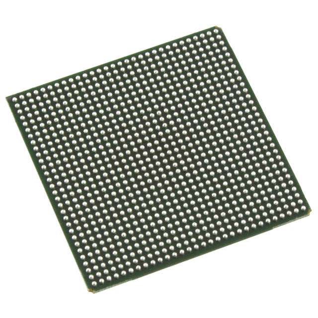
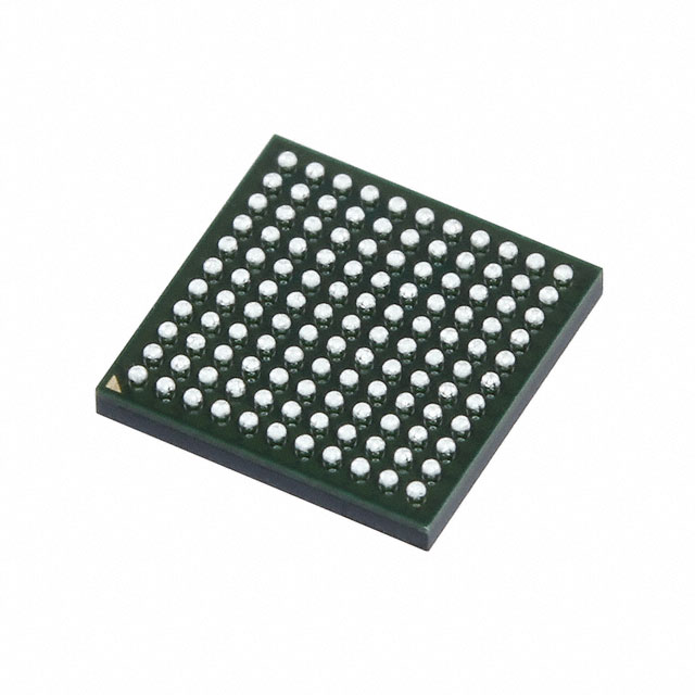
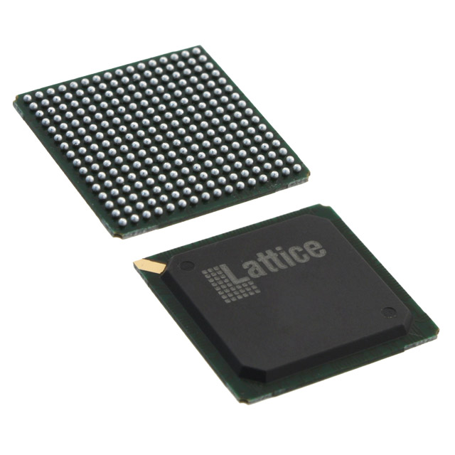
LFSC3GA25E-6F900C
Compare
LFSC3GA25E-6F900C
IC FPGA 378 I/O 900FBGA


Compare
$15.16
Price update:a months ago
Available in stock:
3669


45
Serves customers in 45 countries
1000+
Worldwide Manufacturers
$140M
$140M Growth in 5 Years
50.0M+
50M Parts Shipped in 5 Years

Lattice Semiconductor Corporation
Lattice Semiconductor leads in low-power programmability, solving complex challenges across networks, from Edge to Cloud. With a foothold in communication, computing, industry, autos, and consumers, they nurture lasting relationships, offering world-class support for unfettered innovation, crafting a secure, connected world.
View All Product from Lattice Semiconductor Corporation


Feature
■ High Performance FPGA Fabric
• 15K to 115K four input Look-up Tables (LUT4s)
• 139 to 942 I/Os
• 700MHz global clock; 1GHz edge clocks
■ 4 to 32 High Speed SERDES and flexiPCS™ (per Device)
• Performance ranging from 600Mbps to 3.8Gbps
• Excellent Rx jitter tolerance (0.8UI at 3.125Gbps)
• Low Tx jitter (0.25UI typical at 3.125Gbps)
• Built-in Pre-emphasis and equalization
• Low power (typically 105mW per channel)
• Embedded Physical Coding Sublayer (PCS) provides pre-engineered implementation for the following standards:
– GbE, XAUI, PCI Express, SONET, Serial RapidIO, 1G Fibre Channel, 2G Fibre Channel
■ 2Gbps High Performance PURESPEED™ I/O
• Supports the following performance bandwidths
– Differential I/O up to 2Gbps DDR (1GHz Clock)
– Single-ended memory interfaces up to 800Mbps
• 144 Tap programmable Input Delay (INDEL) block on every I/O dynamically aligns data to clock for robust performance
– Dynamic bit Adaptive Input Logic (AIL) monitoring and control circuitry per pin that automatically ensures proper set-up and hold
– Dynamic bus: uses control bus from DLL
– Static per bit
• Electrical standards supported:
– LVCMOS 3.3/2.5/1.8/1.5/1.2, LVTTL
– SSTL 3/2/18 I, II; HSTL 18/15 I, II
– PCI, PCI-X
– LVDS, Mini-LVDS, Bus-LVDS, MLVDS, LVPECL, RSDS, Hypertransport
• Programmable On Die Termination (ODT)
– Includes Thevenin Equivalent and low power VTT termination options
■ sysCLOCK™ Network
• Eight analog PLLs per device
– Frequency range from 15MHz to 1GHz
– Spread spectrum support
• 12 DLLs per device with direct control of I/O delay
– Frequency range from 100MHz to 700MHz
• Extensive clocking network
– 700MHz primary and 325 MHz secondary clocks
– 1GHz I/O-connected edge clocks
• Precision Clock Divider
– Phase matched x2 and x4 division of incoming clocks
• Dynamic Clock Select (DCS)
– Glitch free clock MUX
■ Masked Array for Cost Optimization (MACO™) Blocks
• On-chip structured ASIC Blocks provide preengineered IP for low power, low cost system level integration
■ High Performance System Bus
• Ties FPGA elements together with a standard bus framework
– Connects to peripheral user interfaces for run-time dynamic configuration
■ System Level Support
• IEEE standard 1149.1 Boundary Scan, plus ispTRACY™ internal logic analyzer
• IEEE Standard 1532 in-system configuration
• 1.2V and 1.0V operation
• Onboard oscillator for initialization and general use
• Embedded PowerPC microprocessor interface
• Low cost wire-bond and high pin count flip-chip packaging
• Low cost SPI Flash RAM configuration


Related Products
| Mfr Part # | Price ($) | Quantity Available | |
|---|---|---|---|
 LFECP6E-3FN484CIC FPGA 224 I/O 484FBGA | Price negotiable |
2327
Marketplace |
Product Attributes
| TYPE | DESCRIPTION | Select all |
|---|---|---|
| Voltage - Supply | 0.95V ~ 1.26V | |
| Mounting Type | Surface Mount | |
| Series | SC | |
| Operating Temperature | 0°C ~ 85°C (TJ) | |
| Package | Tray | |
| Package / Case | 900-BBGA | |
| Product Status | Obsolete | |
| Supplier Device Package | 900-FPBGA (31x31) | |
| Programmable | Not Verified | |
| Number of LABs/CLBs | 6250 | |
| Number of Logic Elements/Cells | 25000 | |
| Total RAM Bits | 1966080 | |
| Number of I/O | 378 |
Blog


 Unveiling the Future: The Surge of Microcontrollers in 2024In the dynamic world of electronic components, microcontrollers stand out as a testament to innovation and versatility. As we edge closer to 2024, the landscape for microcontrollers and semiconductors, spearheaded by giants like STMicroelectronics, Texas Instruments, and Microchip, is set for remarkable transformation.
 Microcontrollers vs. Microprocessors: Unveiling the Core Differences for Embedded Systems EngineeringSeasoned professionals in the realm of embedded systems engineering and product development within the electronics sphere often grapple with distinguishing between microcontrollers and microprocessors. Despite their foundational role in the design and fabrication of a myriad of electronic gadgets, understanding their unique functionalities based on mere definitions can be challenging:
 A Deep Dive into the Global Ceramic Capacitors MarketJoin us in exploring the emerging subplot of environmental consciousness within the global ceramic capacitors market.
 Mastering Current Measurement with MicrocontrollersUnlock precise current measurement secrets with Microcontrollers! Conquer challenges, meet superhero solutions, and revolutionize accuracy with on-chip Analog Core Independent Peripherals (CIPs).
 What is a Rectifier Diode: A Guide to BeginnersMeet the unsung heroes of electronics—Rectifier Diodes! Explore their magic, applications, and join the behind-the-scenes adventure into gadget power.


$15.16
Price update:a months ago
Available in stock:
3669
Lattice Semiconductor Corporation
Lattice Semiconductor leads in low-power programmability, solving complex challenges across networks, from Edge to Cloud. With a foothold in communication, computing, industry, autos, and consumers, they nurture lasting relationships, offering world-class support for unfettered innovation, crafting a secure, connected world.
View All Product from Lattice Semiconductor CorporationBlog
- Unveiling the Future: The Surge of Microcontrollers in 2024In the dynamic world of electronic components, microcontrollers stand out as a testament to innovation and versatility. As we edge closer to 2024, the landscape for microcontrollers and semiconductors, spearheaded by giants like STMicroelectronics, Texas Instruments, and Microchip, is set for remarkable transformation.
- Microcontrollers vs. Microprocessors: Unveiling the Core Differences for Embedded Systems EngineeringSeasoned professionals in the realm of embedded systems engineering and product development within the electronics sphere often grapple with distinguishing between microcontrollers and microprocessors. Despite their foundational role in the design and fabrication of a myriad of electronic gadgets, understanding their unique functionalities based on mere definitions can be challenging:
- A Deep Dive into the Global Ceramic Capacitors MarketJoin us in exploring the emerging subplot of environmental consciousness within the global ceramic capacitors market.
- Mastering Current Measurement with MicrocontrollersUnlock precise current measurement secrets with Microcontrollers! Conquer challenges, meet superhero solutions, and revolutionize accuracy with on-chip Analog Core Independent Peripherals (CIPs).
- What is a Rectifier Diode: A Guide to BeginnersMeet the unsung heroes of electronics—Rectifier Diodes! Explore their magic, applications, and join the behind-the-scenes adventure into gadget power.
Popular Manufacturers
View all manufactures More


Popular Parts Number
More Electronic Parts More
LCMXO1200C-4TN100C
IC FPGA 73 I/O 100TQFP
LFE2M20E-5FN484I
IC FPGA 304 I/O 484FBGA
LCMXO2-1200HC-6MG132C
IC FPGA 104 I/O 132CSBGA
LIFCL-40-7MG121C
IC FPGA 72 I/O 121CSFBGA
LFE2M20E-6FN256C
IC FPGA 140 I/O 256FBGA
ICE40HX1K-CB132
IC FPGA 95 I/O 132CSBGA
LCMXO3LF-2100E-5MG256C
IC FPGA 206 I/O 256CSFBGA
LFD2NX-17-9MG121I
IC FPGA CERTUS-NX 121BGA
LIFCL-40-9MG121I
IC FPGA 72 I/O 121CSFBGA
ICE5LP2K-SG48ITR
IC FPGA 39 I/O 48QFN