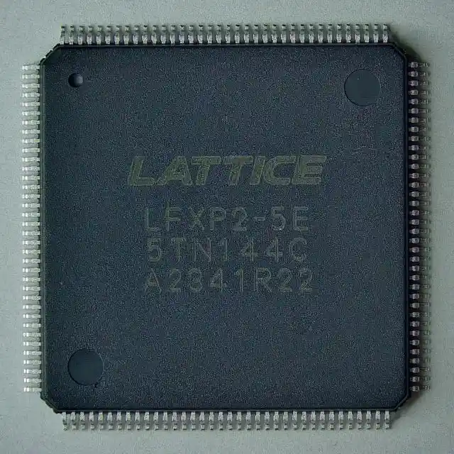
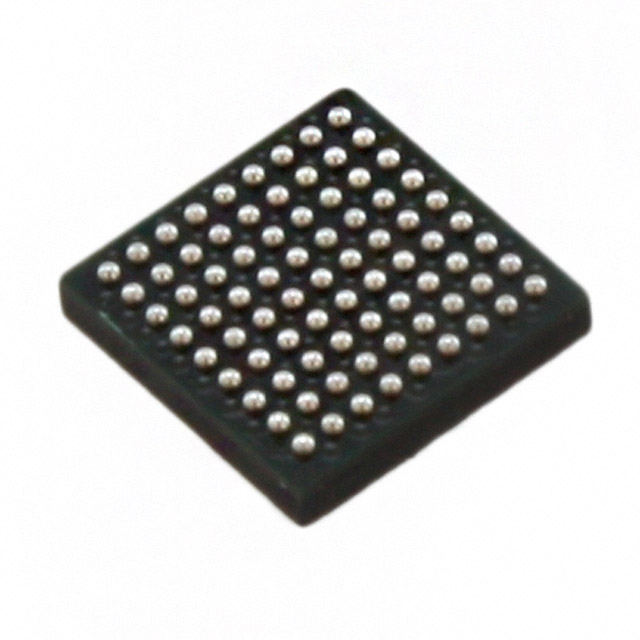
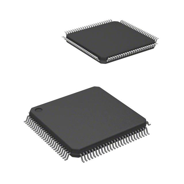
LFXP2-5E-5TN144C
Compare
LFXP2-5E-5TN144C
IC FPGA 100 I/O 144TQFP


Compare
$6.92
Price update:a months ago
Available in stock:
6700


45
Serves customers in 45 countries
1000+
Worldwide Manufacturers
$140M
$140M Growth in 5 Years
50.0M+
50M Parts Shipped in 5 Years

Lattice Semiconductor Corporation
Lattice Semiconductor leads in low-power programmability, solving complex challenges across networks, from Edge to Cloud. With a foothold in communication, computing, industry, autos, and consumers, they nurture lasting relationships, offering world-class support for unfettered innovation, crafting a secure, connected world.
View All Product from Lattice Semiconductor Corporation


_tmb.jpg)
Feature
flexiFLASH™ Architecture
• Instant-on
• Infinitely reconfigurable
• Single chip
• FlashBAK™ technology
• Serial TAG memory
• Design security
Live Update Technology
• TransFR™ technology
• Secure updates with 128 bit AES encryption
• Dual-boot with external SPI
sysDSP™ Block
• Three to eight blocks for high performance Multiply and Accumulate
• 12 to 32 18x18 multipliers
• Each block supports one 36x36 multiplier or four 18x18 or eight 9x9 multipliers
Embedded and Distributed Memory
• Up to 885 Kbits sysMEM™ EBR
• Up to 83 Kbits Distributed RAM
sysCLOCK™ PLLs
• Up to four analog PLLs per device
• Clock multiply, divide and phase shifting
Flexible I/O Buffer
• sysIO™ buffer supports:
– LVCMOS 33/25/18/15/12; LVTTL
– SSTL 33/25/18 class I, II
– HSTL15 class I; HSTL18 class I, II
– PCI
– LVDS, Bus-LVDS, MLVDS, LVPECL, RSDS
Pre-engineered Source Synchronous Interfaces
• DDR / DDR2 interfaces up to 200 MHz
• 7:1 LVDS interfaces support display applications
• XGMII
Density And Package Options
• 5k to 40k LUT4s, 86 to 540 I/Os
• csBGA, TQFP, PQFP, ftBGA and fpBGA packages
• Density migration supported
Flexible Device Configuration
• SPI (master and slave) Boot Flash Interface
• Dual Boot Image supported
• Soft Error Detect (SED) macro embedded
System Level Support
• IEEE 1149.1 and IEEE 1532 Compliant
• On-chip oscillator for initialization & general use
• Devices operate with 1.2V power supply


Related Products
| Mfr Part # | Price ($) | Quantity Available | |
|---|---|---|---|
 LFXP2-5E-5QN208CIC FPGA 146 I/O 208QFP | 7.88 |
6000
Marketplace | |
 LFXP2-5E-5MN132IIC FPGA 86 I/O 132CSBGA | 62.24 |
600
Marketplace | |
LFXP2-5E-5MN132CIC FPGA 86 I/O 132CSBGA | 20.75 |
3600
Marketplace | |
LFXP2-5E-5QN208IIC FPGA 146 I/O 208QFP | 5.19 |
120
Marketplace |
Product Attributes
| TYPE | DESCRIPTION | Select all |
|---|---|---|
| Voltage - Supply | 1.14V ~ 1.26V | |
| Mounting Type | Surface Mount | |
| Series | XP2 | |
| Operating Temperature | 0°C ~ 85°C (TJ) | |
| Package | Tray | |
| Package / Case | 144-LQFP | |
| Product Status | Active | |
| Supplier Device Package | 144-TQFP (20x20) | |
| Programmable | Not Verified | |
| Number of LABs/CLBs | 625 | |
| Number of Logic Elements/Cells | 5000 | |
| Total RAM Bits | 169984 | |
| Number of I/O | 100 |
Blog


 Unveiling the Future: The Surge of Microcontrollers in 2024In the dynamic world of electronic components, microcontrollers stand out as a testament to innovation and versatility. As we edge closer to 2024, the landscape for microcontrollers and semiconductors, spearheaded by giants like STMicroelectronics, Texas Instruments, and Microchip, is set for remarkable transformation.
 Microcontrollers vs. Microprocessors: Unveiling the Core Differences for Embedded Systems EngineeringSeasoned professionals in the realm of embedded systems engineering and product development within the electronics sphere often grapple with distinguishing between microcontrollers and microprocessors. Despite their foundational role in the design and fabrication of a myriad of electronic gadgets, understanding their unique functionalities based on mere definitions can be challenging:
 A Deep Dive into the Global Ceramic Capacitors MarketJoin us in exploring the emerging subplot of environmental consciousness within the global ceramic capacitors market.
 Mastering Current Measurement with MicrocontrollersUnlock precise current measurement secrets with Microcontrollers! Conquer challenges, meet superhero solutions, and revolutionize accuracy with on-chip Analog Core Independent Peripherals (CIPs).
 What is a Rectifier Diode: A Guide to BeginnersMeet the unsung heroes of electronics—Rectifier Diodes! Explore their magic, applications, and join the behind-the-scenes adventure into gadget power.


$6.92
Price update:a months ago
Available in stock:
6700
Lattice Semiconductor Corporation
Lattice Semiconductor leads in low-power programmability, solving complex challenges across networks, from Edge to Cloud. With a foothold in communication, computing, industry, autos, and consumers, they nurture lasting relationships, offering world-class support for unfettered innovation, crafting a secure, connected world.
View All Product from Lattice Semiconductor CorporationBlog
- Unveiling the Future: The Surge of Microcontrollers in 2024In the dynamic world of electronic components, microcontrollers stand out as a testament to innovation and versatility. As we edge closer to 2024, the landscape for microcontrollers and semiconductors, spearheaded by giants like STMicroelectronics, Texas Instruments, and Microchip, is set for remarkable transformation.
- Microcontrollers vs. Microprocessors: Unveiling the Core Differences for Embedded Systems EngineeringSeasoned professionals in the realm of embedded systems engineering and product development within the electronics sphere often grapple with distinguishing between microcontrollers and microprocessors. Despite their foundational role in the design and fabrication of a myriad of electronic gadgets, understanding their unique functionalities based on mere definitions can be challenging:
- A Deep Dive into the Global Ceramic Capacitors MarketJoin us in exploring the emerging subplot of environmental consciousness within the global ceramic capacitors market.
- Mastering Current Measurement with MicrocontrollersUnlock precise current measurement secrets with Microcontrollers! Conquer challenges, meet superhero solutions, and revolutionize accuracy with on-chip Analog Core Independent Peripherals (CIPs).
- What is a Rectifier Diode: A Guide to BeginnersMeet the unsung heroes of electronics—Rectifier Diodes! Explore their magic, applications, and join the behind-the-scenes adventure into gadget power.
Popular Manufacturers
View all manufactures More


Popular Parts Number
More Electronic Parts MoreLFXP2-5E-5TN144C
IC FPGA 100 I/O 144TQFP
ICE40HX4K-BG121
IC FPGA 93 I/O 121CABGA
LCMXO2-7000HC-6TG144C
IC FPGA 114 I/O 144TQFP
LCMXO3LF-1300E-5UWG36ITR1K
IC FPGA 28 I/O 36WLCSP
ICE40LP1K-CM81
IC FPGA 63 I/O 81UCBGA

ICE5LP4K-SWG36ITR1K
IC FPGA 26 I/O 36WLCSP
LCMXO256C-5TN100C
IC FPGA 78 I/O 100TQFP
LCMXO2-1200UHC-4FTG256I
IC FPGA 206 I/O 256FTBGA
LFE5U-25F-8BG381C
IC FPGA 197 I/O 381CABGA
LCMXO1200C-4TN100C
IC FPGA 73 I/O 100TQFP