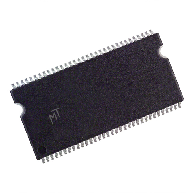
MT46V64M8P-5B IT:J
Compare
MT46V64M8P-5B IT:J
IC DRAM 512MBIT PARALLEL 66TSOP


Compare
$8.27
Price update:a months ago
Available in stock:
2553


45
Serves customers in 45 countries
1000+
Worldwide Manufacturers
$140M
$140M Growth in 5 Years
50.0M+
50M Parts Shipped in 5 Years

Micron Technology Inc.
Micron pioneers inventive solutions driving tech breakthroughs like AI, IoT, self-driving cars, and space exploration. Innovating data management revolutionizes global progress. Over 40 years, 40,000 patents contributed. A diverse team of 34,000 spans 18 nations, fostering inclusive brilliance.
View All Product from Micron Technology Inc.


The MT46V64M8P-5B L IT F of DDR SDRAM uses a double data rate architecture to achieve high-speed operation. The double data rate architecture is essentially a 2n-prefetch architecture with an interface designed to transfer two data words per clock cycle at the I/O pins. A single read or write access for the DDR SDRAM effectively consists of a single 2n-bit-wide, one-clockcycle data transfer at the internal DRAM core and two corresponding n-bit-wide, onehalf-clock-cycle data transfers at the I/O pins. A bidirectional data strobe (DQS) is transmitted externally, along with data, for use in data capture at the receiver. DQS is a strobe transmitted by the DDR SDRAM during READs and by the memory controller during WRITEs. DQS is edge-aligned with data for READs and center-aligned with data for WRITEs. The x16 offering has two data strobes, one for the lower byte and one for the upper byte.
The MT46V64M8P-5B L IT F operates from a differential clock (CK and CK#); the crossing of CK going HIGH and CK# going LOW will be referred to as the positive edge of CK. Commands (address and control signals) are registered at every positive edge of CK. Input data is registered on both edges of DQS, and output data is referenced to both edges of DQS, as well as to both edges of CK. Read and write accesses to the MT46V64M8P-5B L IT F are burst oriented; accesses start at a selected location and continue for a programmed number of locations in a programmed sequence. Accesses begin with the registration of an ACTIVE command, which may then be followed by a READ or WRITE command. The address bits registered coincident with the ACTIVE command are used to select the bank and row to be accessed. The address bits registered coincident with the READ or WRITE command are used to select the bank and the starting column location for the burst access. The DDR SDRAM provides for programmable READ or WRITE burst lengths of 2, 4, or 8 locations.
An auto precharge function may be enabled to provide a self-timed row precharge that is initiated at the end of the burst access. As with standard SDR SDRAMs, the pipelined, multibank architecture of DDR SDRAMs allows for concurrent operation, thereby providing high effective bandwidth by hiding row precharge and activation time. An auto refresh mode is provided, along with a power-saving power-down mode. All inputs are compatible with the JEDEC standard for SSTL_2. All full-drive option outputs are SSTL_2, Class II compatible.
Feature
•VDD= +2.5V ±0.2V, VDDQ = +2.5V ±0.2V
• Bidirectional data strobe (DQS) transmitted/ received with data, i.e., source-synchronous data
capture (x16 has two – one per byte)
• Internal, pipelined double-data-rate (DDR) architecture; two data accesses per clock cycle
• Differential clock inputs (CK and CK#)
• Commands entered on each positive CK edge
• DQS edge-aligned with data for READs; center aligned with data for WRITEs
• DLL to align DQ and DQS transitions with CK
• Four internal banks for concurrent operation
• Data mask (DM) for masking write data (x16 has two – one per byte)
• Programmable burst lengths: 2, 4, or 8
• x16 has programmable IOL/IOV.
• Concurrent auto precharge option is supported
• Auto Refresh and Self Refresh Modes
• Longer lead TSOP for improved reliability (OCPL)
• 2.5V I/O (SSTL_2 compatible)


Related Products
| Mfr Part # | Price ($) | Quantity Available | |
|---|---|---|---|
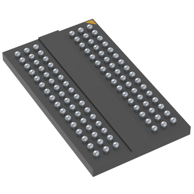
 MT46V64M8FN-5B:D TRIC DRAM 512MBIT PARALLEL 60FBGA | 2.20 |
4286
Marketplace |
Product Attributes
| TYPE | DESCRIPTION | Select all |
|---|---|---|
| Memory Type | Volatile | |
| Programmable | Not Verified | |
| Access Time | 700 ps | |
| Write Cycle Time - Word, Page | 15ns | |
| Clock Frequency | 200 MHz | |
| Product Status | Obsolete | |
| Memory Interface | Parallel | |
| Package | Box | |
| Memory Organization | 64M x 8 | |
| Memory Size | 512Mbit | |
| Technology | SDRAM - DDR | |
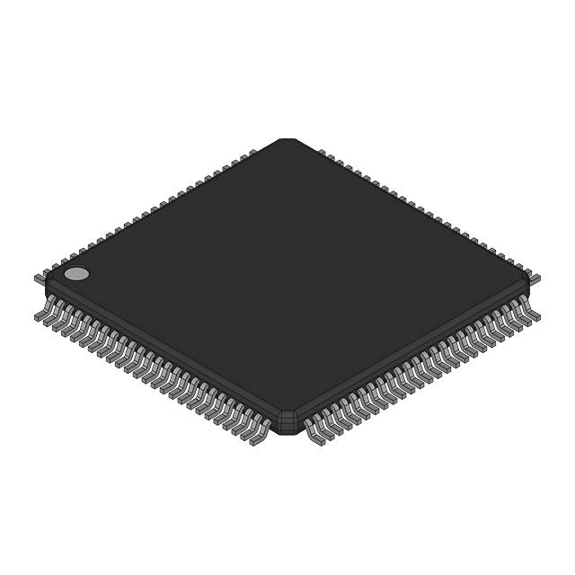
| Supplier Device Package | 66-TSOP | |
| Memory Format | DRAM | |
| Package / Case | 66-TSSOP (0.400", 10.16mm Width) | |
| Mounting Type | Surface Mount | |
| Operating Temperature | -40°C ~ 85°C (TA) | |
| Voltage - Supply | 2.5V ~ 2.7V |
Blog


 Unveiling the Future: The Surge of Microcontrollers in 2024In the dynamic world of electronic components, microcontrollers stand out as a testament to innovation and versatility. As we edge closer to 2024, the landscape for microcontrollers and semiconductors, spearheaded by giants like STMicroelectronics, Texas Instruments, and Microchip, is set for remarkable transformation.
 Microcontrollers vs. Microprocessors: Unveiling the Core Differences for Embedded Systems EngineeringSeasoned professionals in the realm of embedded systems engineering and product development within the electronics sphere often grapple with distinguishing between microcontrollers and microprocessors. Despite their foundational role in the design and fabrication of a myriad of electronic gadgets, understanding their unique functionalities based on mere definitions can be challenging:
 A Deep Dive into the Global Ceramic Capacitors MarketJoin us in exploring the emerging subplot of environmental consciousness within the global ceramic capacitors market.
 Mastering Current Measurement with MicrocontrollersUnlock precise current measurement secrets with Microcontrollers! Conquer challenges, meet superhero solutions, and revolutionize accuracy with on-chip Analog Core Independent Peripherals (CIPs).
 What is a Rectifier Diode: A Guide to BeginnersMeet the unsung heroes of electronics—Rectifier Diodes! Explore their magic, applications, and join the behind-the-scenes adventure into gadget power.


$8.27
Price update:a months ago
Available in stock:
2553
Micron Technology Inc.
Micron pioneers inventive solutions driving tech breakthroughs like AI, IoT, self-driving cars, and space exploration. Innovating data management revolutionizes global progress. Over 40 years, 40,000 patents contributed. A diverse team of 34,000 spans 18 nations, fostering inclusive brilliance.
View All Product from Micron Technology Inc.Blog
- Unveiling the Future: The Surge of Microcontrollers in 2024In the dynamic world of electronic components, microcontrollers stand out as a testament to innovation and versatility. As we edge closer to 2024, the landscape for microcontrollers and semiconductors, spearheaded by giants like STMicroelectronics, Texas Instruments, and Microchip, is set for remarkable transformation.
- Microcontrollers vs. Microprocessors: Unveiling the Core Differences for Embedded Systems EngineeringSeasoned professionals in the realm of embedded systems engineering and product development within the electronics sphere often grapple with distinguishing between microcontrollers and microprocessors. Despite their foundational role in the design and fabrication of a myriad of electronic gadgets, understanding their unique functionalities based on mere definitions can be challenging:
- A Deep Dive into the Global Ceramic Capacitors MarketJoin us in exploring the emerging subplot of environmental consciousness within the global ceramic capacitors market.
- Mastering Current Measurement with MicrocontrollersUnlock precise current measurement secrets with Microcontrollers! Conquer challenges, meet superhero solutions, and revolutionize accuracy with on-chip Analog Core Independent Peripherals (CIPs).
- What is a Rectifier Diode: A Guide to BeginnersMeet the unsung heroes of electronics—Rectifier Diodes! Explore their magic, applications, and join the behind-the-scenes adventure into gadget power.
Popular Manufacturers
View all manufactures More


Popular Parts Number
More Electronic Parts More
MT29F4G08ABADAWP-AATX:D TR
IC FLASH 4GBIT PARALLEL 48TSOP I

MT25QL256ABA8E12-0AUT TR
IC FLASH 256MBIT SPI 24TPBGA

MT53E256M32D2FW-046 AUT:B
LPDDR4 8G 256MX32 FBGA DDP
MT41K512M16VRN-107 AIT:P TR
IC DRAM 8GBIT PAR 96FBGA

MT62F2G32D4DS-023 AAT:B TR
LPDDR5 64G 2GX32 FBGA
MT53E1G32D2FW-046 IT:A TR
LPDDR4 32G 1GX32 FBGA DDP
MT46H128M16LFDD-48 IT:C
IC DRAM 2GBIT PAR 208MHZ 60VFBGA
MT53D1024M32D4DT-053 AAT:D
IC DRAM 32GBIT 1.866GHZ 200VFBGA
MT25QL128ABA8E12-0AAT TR
IC FLASH 128MBIT SPI 24TPBGA
MT58L64L32PT-7.5
IC SRAM 2MBIT PARALLEL 100TQFP