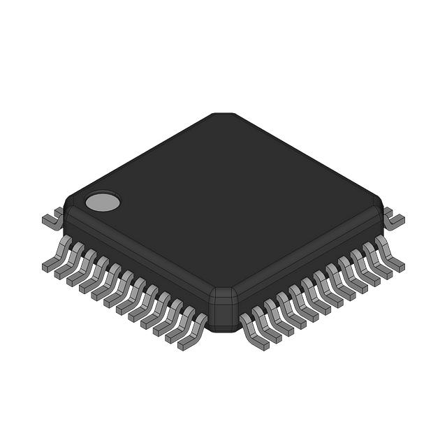
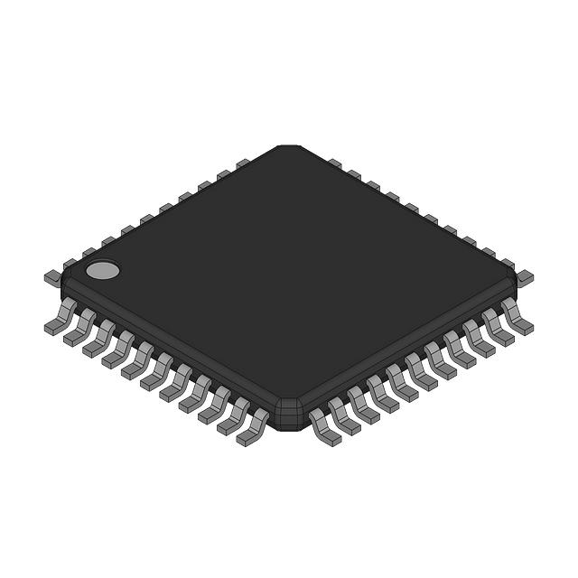
MC9S12C32CFAE16
Compare
MC9S12C32CFAE16
IC MCU 16BIT 32KB FLASH 48LQFP


Compare
$165.36
Price update:a months ago
Available in stock:
44


45
Serves customers in 45 countries
1000+
Worldwide Manufacturers
$140M
$140M Growth in 5 Years
50.0M+
50M Parts Shipped in 5 Years

NXP USA Inc.
NXP Semiconductors, a frontrunner in embedded controllers, offers a wide array of MCUs with Arm-based processors. Their innovation extends to robust Power Management for industry and automotive use. NXP's products globally empower and interconnect, fostering proficiency for individuals, organizations, and the world. Noteworthy is the integration of Freescale Semiconductor into NXP (December 2015).
View All Product from NXP USA Inc.


Based on NXP/FREESCALE/Motorola's market-leading flash technology, The MC9S12C32CFAE16 MCU chip is the members of the MC9S12C-Family deliver the power and flexibility of our 16 Bit core (CPU12) family to a whole new range of cost and space sensitive, general purpose Industrial and Automotive network applications.
The MC9S12C32CFAE16 device is comprised of standard on-chip peripherals including a 16-bit central processing unit (CPU12), up to 128K bytes of Flash EEPROM or ROM, up to 4K bytes of RAM, an asynchronous serial communications in terface (SCI), a serial peripheral interface (SPI), an 8-channel 16-bit timer module (TIM), a 6-channel 8-bit Pulse Width Modulator (PWM), an 8-channel, 10-bit analog-to-digital converter (ADC) and up to one CAN 2.0 A, B software compatible module (MSCAN12).
The C-Family includes ROM versions MC3S12C128/96/64/32/16 of all devices which provide a further cost reduction path for applications with high volume and stable code.
Feature
• 16-bit HCS12 CORE
— HCS12 CPU
— MMC (memory map and interface)
— INT (interrupt control)
— BDM (background debug mode)
— DBG12 (enhanced debug12 module including breakpoints and change-of-flow trace buffer)
— Multiplexed Expansion Bus (available only in 80 pin package version)
• 16-bit HCS12 CPU
— Upward compatible with M68HC11 instruction set
— Interrupt stacking and programmer’s model identical to M68HC11
— Instruction queue
— Enhanced indexed addressing
• Wake-up interrupt inputs
— Up to 10-port bits available for wake up interrupt function
• Memory options
— 16K, 32K, 64K, 96K and 128K Byte Flash EEPROM (erasable in 512-byte sectors) or
— 16K, 32K, 64K, 96K and 128K Byte ROM
— 2K and 4K Byte RAM
• Analog-to-Digital Converters
— One 8-channel module with 10-bit resolution.
— External conversion trigger capability
• Up to one 1M bit per second, CAN 2.0 A, B software compatible modules
— Five receive and three transmit buffers
— Flexible identifier filter programmable as 2 x 32 bit, 4 x 16 bit or 8 x 8 bit
— Four separate interrupt channels for receive, transmit, error and wake-up
— Low-pass filter wake-up function
— Loop-back for self test operation
• Timer Module (TIM)
— 16-bit Counter with 7-bit Prescaler
— 8 programmable input capture or output compare channels
— Simple PWM Mode
— Modulo Reset of Timer Counter
— 16-Bit Pulse Accumulator
— External Event Counting
— Gated Time Accumulation
• 6 PWM channels
— Programmable period and duty cycle
— 8-bit 6-channel or 16-bit 3-channel
— Separate control for each pulse width and duty cycle
— Center-aligned or left-aligned outputs
— Programmable clock select logic with a wide range of frequencies
— Fast emergency shutdown input
• Serial interfaces
— One asynchronous serial communications interface (SCI)
— One synchronous serial peripheral interface (SPI)
• CRG (Clock Reset Generator Module)
— Windowed COP watchdog,
— Real time interrupt,
— Clock monitor,
— Clock generation
— Reset Generation
— Phase-locked loop clock frequency multiplier
— Limp home mode in absence of external clock
— Low power 0.5 to 16 MHz crystal oscillator reference clock
• Operation frequency
— 32MHz equivalent to 16MHz Bus Speed for single chip
— 32MHz equivalent to 16MHz Bus Speed in expanded bus modes
— Option: 50MHz equivalent to 25MHz Bus Speed
• Internal 2.5V Regulator
— Supports an input voltage range from 3.3V-10% to 5.5V
— Low power mode capability
— Includes low voltage reset (LVR) circuitry
— Includes low voltage interrupt (LVI) circuitry
• 48-Pin LQFP, 52-Pin LQFP or 80-Pin QFP package
— Up to 58 I/O lines with 5V input and drive capability
— Up to 2 dedicated 5V input only lines (IRQ, XIRQ)
— 5V A/D converter inputs and 5V I/O
• Development support
— Single-wire background debug™ mode (BDM)
— On-chip hardware breakpoints
— Enhanced DBG12 debug features


Related Products
| Mfr Part # | Price ($) | Quantity Available | |
|---|---|---|---|
 MC9S12C128CPBEIC MCU 16BIT 128KB FLASH 52TQFP | 15.03 |
8366
Marketplace | |
 MC9S12C128VFUEIC MCU 16BIT 128KB FLASH 80QFP | 137.80 |
2375
Marketplace | |
 MC9S12B64CPVEIC MCU 16BIT 64KB FLASH 112LQFP | Price negotiable |
3475
Marketplace | |
 MC9S12B64MPVEIC MCU 16BIT 64KB FLASH 112LQFP | 19.01 |
300
Marketplace | |
 MC9S12C128CPBEIC MCU 16BIT 128KB FLASH 52TQFP | 4.13 |
2335
Marketplace | |
 MC9S12C128VFUEIC MCU 16BIT 128KB FLASH 80QFP | 18.94 |
4537
Marketplace | |
 MC9S12B64CPVEIC MCU 16BIT 64KB FLASH 112LQFP | 13.67 |
173
Marketplace | |
MC9S12B64MPVEIC MCU 16BIT 64KB FLASH 112LQFP | 18.19 |
3031
Marketplace |
-
MC9S12C128CPBE
IC MCU 16BIT 128KB FLASH 52TQFP
-
MC9S12C128VFUE
IC MCU 16BIT 128KB FLASH 80QFP
-
MC9S12B64CPVE
IC MCU 16BIT 64KB FLASH 112LQFP
-
MC9S12B64MPVE
IC MCU 16BIT 64KB FLASH 112LQFP
-
MC9S12C128CPBE
IC MCU 16BIT 128KB FLASH 52TQFP
-
MC9S12C128VFUE
IC MCU 16BIT 128KB FLASH 80QFP
-
MC9S12B64CPVE
IC MCU 16BIT 64KB FLASH 112LQFP
-
MC9S12B64MPVE
IC MCU 16BIT 64KB FLASH 112LQFP
Product Attributes
| TYPE | DESCRIPTION | Select all |
|---|---|---|
| Voltage - Supply (Vcc/Vdd) | 2.35V ~ 5.5V | |
| Core Processor | HCS12 | |
| Data Converters | A/D 8x10b | |
| Core Size | 16-Bit | |
| Oscillator Type | Internal | |
| Speed | 16MHz | |
| Operating Temperature | -40°C ~ 85°C (TA) | |
| Connectivity | CANbus, EBI/EMI, SCI, SPI | |
| Mounting Type | Surface Mount | |
| Peripherals | POR, PWM, WDT | |
| Package / Case | 48-LQFP | |
| Number of I/O | 31 | |
| Supplier Device Package | 48-LQFP (7x7) | |
| Program Memory Size | 32KB (32K x 8) | |
| Program Memory Type | FLASH | |
| RAM Size | 2K x 8 | |
| Programmable | Not Verified | |
| Series | HCS12 | |
| Package | Bulk | |
| Product Status | Active |
Blog


 Unveiling the Future: The Surge of Microcontrollers in 2024In the dynamic world of electronic components, microcontrollers stand out as a testament to innovation and versatility. As we edge closer to 2024, the landscape for microcontrollers and semiconductors, spearheaded by giants like STMicroelectronics, Texas Instruments, and Microchip, is set for remarkable transformation.
 Microcontrollers vs. Microprocessors: Unveiling the Core Differences for Embedded Systems EngineeringSeasoned professionals in the realm of embedded systems engineering and product development within the electronics sphere often grapple with distinguishing between microcontrollers and microprocessors. Despite their foundational role in the design and fabrication of a myriad of electronic gadgets, understanding their unique functionalities based on mere definitions can be challenging:
 A Deep Dive into the Global Ceramic Capacitors MarketJoin us in exploring the emerging subplot of environmental consciousness within the global ceramic capacitors market.
 Mastering Current Measurement with MicrocontrollersUnlock precise current measurement secrets with Microcontrollers! Conquer challenges, meet superhero solutions, and revolutionize accuracy with on-chip Analog Core Independent Peripherals (CIPs).
 What is a Rectifier Diode: A Guide to BeginnersMeet the unsung heroes of electronics—Rectifier Diodes! Explore their magic, applications, and join the behind-the-scenes adventure into gadget power.


$165.36
Price update:a months ago
Available in stock:
44
NXP USA Inc.
NXP Semiconductors, a frontrunner in embedded controllers, offers a wide array of MCUs with Arm-based processors. Their innovation extends to robust Power Management for industry and automotive use. NXP's products globally empower and interconnect, fostering proficiency for individuals, organizations, and the world. Noteworthy is the integration of Freescale Semiconductor into NXP (December 2015).
View All Product from NXP USA Inc.Blog
- Unveiling the Future: The Surge of Microcontrollers in 2024In the dynamic world of electronic components, microcontrollers stand out as a testament to innovation and versatility. As we edge closer to 2024, the landscape for microcontrollers and semiconductors, spearheaded by giants like STMicroelectronics, Texas Instruments, and Microchip, is set for remarkable transformation.
- Microcontrollers vs. Microprocessors: Unveiling the Core Differences for Embedded Systems EngineeringSeasoned professionals in the realm of embedded systems engineering and product development within the electronics sphere often grapple with distinguishing between microcontrollers and microprocessors. Despite their foundational role in the design and fabrication of a myriad of electronic gadgets, understanding their unique functionalities based on mere definitions can be challenging:
- A Deep Dive into the Global Ceramic Capacitors MarketJoin us in exploring the emerging subplot of environmental consciousness within the global ceramic capacitors market.
- Mastering Current Measurement with MicrocontrollersUnlock precise current measurement secrets with Microcontrollers! Conquer challenges, meet superhero solutions, and revolutionize accuracy with on-chip Analog Core Independent Peripherals (CIPs).
- What is a Rectifier Diode: A Guide to BeginnersMeet the unsung heroes of electronics—Rectifier Diodes! Explore their magic, applications, and join the behind-the-scenes adventure into gadget power.
Popular Manufacturers
View all manufactures More


Popular Parts Number
More Electronic Parts More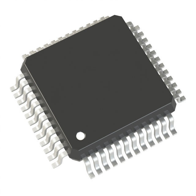
MC9S12C32CFAE16
IC MCU 16BIT 32KB FLASH 48LQFP
S908QY4E0CDWER
MICROCONTROLLER, 8 BIT, HC08/S08

MC9S08RC8FJE
IC MCU 8BIT 8KB FLASH 32LQFP
MC9S08MM32CLH
IC MCU 8BIT 32KB FLASH 64LQFP
MC908GP16CFBE
IC MCU 8BIT 16KB FLASH 44QFP

MCF51AG96VQH
IC MCU 32BIT 96KB FLASH 64QFP
MCF52211CEP66
IC MCU 32BIT 128KB FLASH 64QFN

MC9S08RG32CFJ
8-BIT, FLASH, 8MHZ PQFP32

MC9S08DN60MLF
IC MCU 8BIT 60KB FLASH 48LQFP
S912XET256J1MALR
MICROCONTROLLER, 16 BIT, HCS12 C