All categories
- All categories
- Integrated Circuits (ICs)
- Development Boards, Kits, Programmers
- Discrete Semiconductor Products
- Power Supplies - Board Mount
- RF and Wireless
- Sensors, Transducers
- Memory Cards, Modules
- Audio Products
- Circuit Protection
- Crystals, Oscillators, Resonators
- Filters
- Isolators
- Kits
- Maker/DIY, Educational
- Optoelectronics
- Power Supplies - External/Internal (Off-Board)
- Relays
- Resistors
- Test and Measurement
- Uncategorized
- Connectors, Interconnects
- Inductors, Coils, Chokes
- Motors, Actuators, Solenoids and Drivers
- Switches
- Cable Assemblies
- Embedded Computers
- Capacitors
- Fans, Thermal Management
- Transformers
- Battery Products
- Products
- All categories
-
Integrated Circuits (ICs)
-
Embedded
- FPGAs (Field Programmable Gate Array)
- Microcontrollers
- CPLDs (Complex Programmable Logic Devices)
- FPGAs (Field Programmable Gate Array) with Microcontrollers
- PLDs (Programmable Logic Device)
- Microcontrollers, Microprocessor, FPGA Modules
- System On Chip (SoC)
- Application Specific Microcontrollers
- DSP (Digital Signal Processors)
- Microprocessors
-
Interface
- Drivers, Receivers, Transceivers
- Sensor and Detector Interfaces
- Analog Switches - Special Purpose
- Analog Switches, Multiplexers, Demultiplexers
- CODECS
- Controllers
- Direct Digital Synthesis (DDS)
- Encoders, Decoders, Converters
- Filters - Active
- I/O Expanders
- Modems - ICs and Modules
- Modules
- Sensor, Capacitive Touch
- Signal Buffers, Repeaters, Splitters
- Signal Terminators
- Specialized
- Telecom
- Serializers, Deserializers
- UARTs (Universal Asynchronous Receiver Transmitter)
- Voice Record and Playback
- Memory
-
Power Management (PMIC)
- DC DC Switching Controllers
- Display Drivers
- Full Half-Bridge Drivers
- Gate Drivers
- LED Drivers
- Motor Drivers, Controllers
- Power Distribution Switches, Load Drivers
- Power Management - Specialized
- Power Supply Controllers, Monitors
- Special Purpose Regulators
- Supervisors
- Voltage Regulators - DC DC Switching Regulators
- Voltage Regulators - Linear
- Voltage Regulators - Linear + Switching
- AC DC Converters, Offline Switches
- Battery Chargers
- Battery Management
- Current Regulation/Management
- Energy Metering
- Hot Swap Controllers
- Laser Drivers
- Lighting, Ballast Controllers
- OR Controllers, Ideal Diodes
- PFC (Power Factor Correction)
- Power Over Ethernet (PoE) Controllers
- RMS to DC Converters
- Thermal Management
- Voltage Reference
- Voltage Regulators - Linear Regulator Controllers
- V/F and F/V Converters
- Specialized ICs
- Audio Special Purpose
- Clock/Timing
- Data Acquisition
- Linear
-
Logic
- Buffers, Drivers, Receivers, Transceivers
- Comparators
- FIFOs Memory
- Flip Flops
- Gates and Inverters
- Gates and Inverters - Multi-Function, Configurable
- Multivibrators
- Shift Registers
- Signal Switches, Multiplexers, Decoders
- Translators, Level Shifters
- Latches
- Specialty Logic
- Counters, Dividers
- Parity Generators and Checkers
- Universal Bus Functions
-
Embedded
-
Development Boards, Kits, Programmers
- Accessories
- Evaluation and Demonstration Boards and Kits
- Evaluation Boards - DC/DC & AC/DC (Off-Line) SMPS
- Evaluation Boards - Expansion Boards, Daughter Cards
- Evaluation Boards - LED Drivers
- Evaluation Boards - Sensors
- Evaluation Boards - Embedded - Complex Logic (FPGA, CPLD)
- Evaluation Boards - Embedded - MCU, DSP
- Programmers, Emulators, and Debuggers
- Software, Services
- Evaluation Boards - Analog to Digital Converters (ADCs)
- Evaluation Boards - Audio Amplifiers
- Evaluation Boards - Digital to Analog Converters (DACs)
- Evaluation Boards - Linear Voltage Regulators
- Evaluation Boards - Op Amps
- Programming Adapters, Sockets
- RF Evaluation and Development Kits, Boards
- RFID Evaluation and Development Kits, Boards
-
Discrete Semiconductor Products
- Power Supplies - Board Mount
-
RF and Wireless
- RF Amplifiers
- Attenuators
- RF Accessories
- RF Demodulators
- RF Detectors
- RF Front End (LNA + PA)
- RF Misc ICs and Modules
- RF Mixers
- RF Modulators
- RF Power Controller ICs
- RF Power Dividers/Splitters
- RF Receivers
- RF Shields
- RF Switches
- RF Transceiver ICs
- RF Transceiver Modules and Modems
- RF Transmitters
- RFID, RF Access, Monitoring ICs
- RFID Transponders, Tags
- RF Multiplexers
- RF Receiver, Transmitter, and Transceiver Finished Units
- RF Antennas
- RFI and EMI - Contacts, Fingerstock and Gaskets
- RFID Reader Modules
- RF Circulators and Isolators
- RF Directional Coupler
- Balun
- Subscriber Identification Module (SIM) Cards
- RFID Accessories
- RFID Antennas
-
Sensors, Transducers
- Current Sensors
- Magnetic Sensors
- Position Sensors
- Specialized Sensors
- Temperature Sensors
- Motion Sensors
- Multifunction
-
Optical Sensors
- Ambient Light, IR, UV Sensors
- Image Sensors, Camera
- Photodiodes
- Distance Measuring
- Photointerrupters - Slot Type - Transistor Output
- Phototransistors
- Reflective - Analog Output
- Reflective - Logic Output
- Photo Detectors - Logic Output
- Photointerrupters - Slot Type - Logic Output
- Photoelectric, Industrial
- Camera Modules
- Photo Detectors - Remote Receiver
- Sensor, Transducer Accessories
- Sensor, Transducer Amplifiers
- Color Sensors
- Encoders
- Encoders - Industrial
- Touch Sensors
- Pressure Sensors, Transducers
- Flow Sensors
- Gas Sensors
- Pressure Sensors, Transducers - Industrial
- Float, Level Sensors
- Magnets
- Proximity Sensors
- Flow Sensors - Industrial
- Humidity, Moisture Sensors
- Memory Cards, Modules
- Audio Products
- Circuit Protection
- Crystals, Oscillators, Resonators
- Filters
- Isolators
- Kits
- Maker/DIY, Educational
-
Optoelectronics
- Circuit Board Indicators, Arrays, Light Bars, Bar Graphs
- Fiber Optic Transceiver Modules
- LED Character and Numeric
- COBs, Engines, Modules, Strips
- Color LED Lighting
- Display Bezels, Lenses
- Fiber Optic Receivers
- Fiber Optic Transmitters - Discrete
- Fiber Optic Transmitters - Drive Circuitry Integrated
- Laser Diodes, Modules
- LED Dot Matrix and Cluster
- LED Emitters - Infrared, UV, Visible
- LED Indication - Discrete
- Lenses
- Optoelectronics Accessories
- White LED Lighting
- Incandescent, Neon Lamps
- Fiber Optic Switches, Multiplexers, Demultiplexers
- Ballasts, Inverters
- LCD, OLED, Graphic
- LCD, OLED Character and Numeric
- Display, Monitor - LCD Driver/Controller
- Power Supplies - External/Internal (Off-Board)
- Relays
- Resistors
- Test and Measurement
- Uncategorized
- Connectors, Interconnects
- Inductors, Coils, Chokes
- Motors, Actuators, Solenoids and Drivers
- Switches
- Cable Assemblies
- Embedded Computers
- Capacitors
- Fans, Thermal Management
- Transformers
- Battery Products
- Manufacturers
- Services
- Industries
- Top-Quality Commitment
- Resources
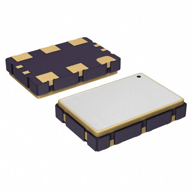
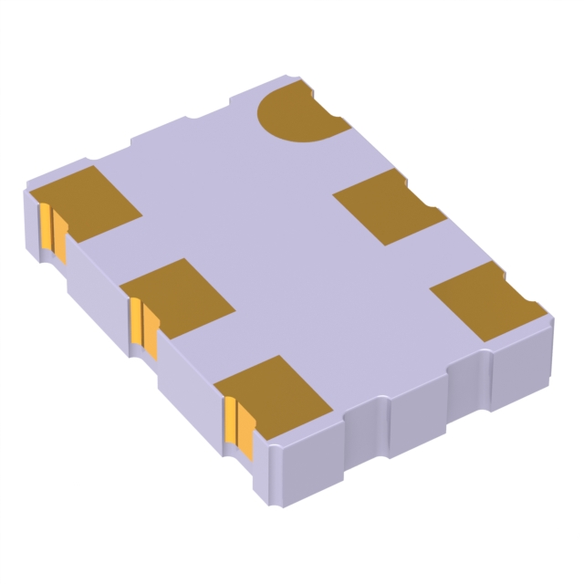
8N3QV01KG-0009CDI8

8N3QV01KG-0009CDI8 datasheet
8N3QV01KG-0009CDI8 pdf
8N3QV01KG-0009CDI8 distributor
8N3QV01KG-0009CDI8 manufacturer
8N3QV01KG-0009CDI8 supplier
8N3QV01KG-0009CDI8 price
8N3QV01KG-0009CDI8 specification
8N3QV01KG-0009CDI8 wholesale
8N3QV01KG-0009CDI8 package
8N3QV01KG-0009CDI8 Renesas Electronics America Inc.
8N3QV01KG-0009CDI8
Compare
8N3QV01KG-0009CDI8
IC OSC VCXO QD FREQ 10CLCC


Compare
Price negotiable
Price update:a months ago
Available in stock:
7584


45
Serves customers in 45 countries
1000+
Worldwide Manufacturers
$140M
$140M Growth in 5 Years
50.0M+
50M Parts Shipped in 5 Years

Renesas Electronics America Inc.
Renesas Electronics Corporation pioneers intricate semiconductor solutions, empowering myriad intelligent devices to enhance human lives securely. A global leader in microcontrollers, analog products, and SoCs, Renesas shapes a limitless future across Automotive, Industrial, and ICT domains.
View All Product from Renesas Electronics America Inc.Popular Products
 8N4SV75KC-0183CDI8IC OSC VCXO 644.5313MHZ 6CLCCPrice negotiable Detail
 R5F10AGCLFB#X5IC MCU 16BIT LFQFPPrice negotiable Detail
 HIP2100IR4TIC GATE DRVR HALF-BRIDGE 12DFNPrice negotiable Detail
 XLH73V052.000000XXTAL OSC VCXO 52.0000MHZ HCMOSPrice negotiable Detail
 ISL54410IRUZ-TIC SW USB/AUDIO DUAL SPT 10UTQFN$0.82 Detail
 MPC9653AACR2/WIC PLL CLOCK GENERATOR 32TQFPPrice negotiable Detail
 843202AYILFIC FREQ SYNTH 32TQFPPrice negotiable Detail
 R5F10WMAGFB#10IC MCU 16BIT 16KB FLASH 80LQFP$2.95 Detail
 R5F52306ADNE#U0IC MCU 32BIT 256KB FLASH 48HWQFN$3.37 Detail
- R4F24259DWFAU16-BIT, FLASH, H8S/2600 CPU$10.35 Detail
- CD40105BDMSRRENESASPrice negotiable Detail
 8N3QV01KG-0021CDIIC OSC VCXO QD FREQ 10CLCCPrice negotiable Detail
 9E4101AFILFTIC TIMING CTRL HUB PROG 56SSOPPrice negotiable Detail
- 7016S35JIC SRAM 144KBIT PARALLEL 68PLCCPrice negotiable Detail
 IDT71V2556S133PF8IC SRAM 4.5MBIT PARALLEL 100TQFPPrice negotiable Detail
- 8N4SV75KC-0183CDI8IC OSC VCXO 644.5313MHZ 6CLCCPrice negotiable Detail
- R5F10AGCLFB#X5IC MCU 16BIT LFQFPPrice negotiable Detail
- HIP2100IR4TIC GATE DRVR HALF-BRIDGE 12DFNPrice negotiable Detail
- XLH73V052.000000XXTAL OSC VCXO 52.0000MHZ HCMOSPrice negotiable Detail
- ISL54410IRUZ-TIC SW USB/AUDIO DUAL SPT 10UTQFN$0.82 Detail
- MPC9653AACR2/WIC PLL CLOCK GENERATOR 32TQFPPrice negotiable Detail
- 843202AYILFIC FREQ SYNTH 32TQFPPrice negotiable Detail
- R5F10WMAGFB#10IC MCU 16BIT 16KB FLASH 80LQFP$2.95 Detail
- R5F52306ADNE#U0IC MCU 32BIT 256KB FLASH 48HWQFN$3.37 Detail
- R4F24259DWFAU16-BIT, FLASH, H8S/2600 CPU$10.35 Detail
- CD40105BDMSRRENESASPrice negotiable Detail
- 8N3QV01KG-0021CDIIC OSC VCXO QD FREQ 10CLCCPrice negotiable Detail
- 9E4101AFILFTIC TIMING CTRL HUB PROG 56SSOPPrice negotiable Detail
- 7016S35JIC SRAM 144KBIT PARALLEL 68PLCCPrice negotiable Detail
- IDT71V2556S133PF8IC SRAM 4.5MBIT PARALLEL 100TQFPPrice negotiable Detail
- 8N4SV75KC-0183CDI8IC OSC VCXO 644.5313MHZ 6CLCCPrice negotiable Detail
- R5F10AGCLFB#X5IC MCU 16BIT LFQFPPrice negotiable Detail
- HIP2100IR4TIC GATE DRVR HALF-BRIDGE 12DFNPrice negotiable Detail
- XLH73V052.000000XXTAL OSC VCXO 52.0000MHZ HCMOSPrice negotiable Detail
- ISL54410IRUZ-TIC SW USB/AUDIO DUAL SPT 10UTQFN$0.82 Detail
Product Details
Shipping
Package
Quality Guarantee
The 8N3QV01EG-0009CDI8 is a Quad-Frequency Programmable VCXO with very flexible frequency and pull-range programming capabilities. The device uses IDT's fourth generation FemtoClock® NG technology for an optimum of high clock frequency and low phase noise performance. The device accepts 2.5V or 3.3V supply and is packaged in a small, lead-free (RoHS 6) 10-lead Ceramic 5mm x 7mm x 1.55mm package. Besides the 4 default power-up frequencies set by the FSEL0 and FSEL1 pins, the 8N3QV01EG-0009CDI8 can be programmed via the I2C interface to any output clock frequency between 15.476MHz to 866.67MHz and from 975MHz to 1,300MHz to a very high degree of precision with a frequency step size of 435.9Hz ÷N (N is the PLL output divider). Since the FSEL0 and FSEL1 pins are mapped to 4 independent PLL M and N divider registers (P, MINT, MFRAC and N), reprogramming those registers to other frequencies under control of FSEL0 and FSEL1 is supported. The extended temperature range supports wireless infrastructure, telecommunication and networking end equipment requirements. The device is a member of the high-performance clock family from IDT.
Feature
- Fourth generation FemtoClock® NG technology
- Programmable clock output frequency from 15.476MHz to 866.67MHz and from 975MHz to 1,300MHz
- Four power-up default frequencies (see part number order codes), reprogrammable by I2C
- I2C programming interface for the output clock frequency, APR and internal PLL control registers
- Frequency programming resolution is 435.9Hz ÷N
- Absolute pull-range (APR) programmable from ±4.5 to ±754.5ppm
- One 2.5V or 3.3V LVPECL differential clock output
- Two control inputs for the power-up default frequency
- LVCMOS/LVTTL compatible control inputs
- RMS phase jitter @ 156.25MHz (12kHz - 20MHz): 0.487ps (typical)
- RMS phase jitter @ 156.25MHz (1kHz - 40MHz): 0.614ps (typical)
- 2.5V or 3.3V supply voltage modes
- -40°C to 85°C ambient operating temperature
- Available in Lead-free (RoHS 6) package
Shipping Cost
- 1. Shipping starts at $40, but prices may vary for certain countries like South Africa, Brazil, India, Pakistan, Israel, etc.
- 2. The basic freight for packages ≤0.5kg or equivalent volume is influenced by the time zone and country.
Shipping Method
- 1. Our products are currently shipped using DHL, SF, and UPS. For low quantities, FedEx is the chosen carrier.
Delivery Time
- 1. Once shipped, the estimated delivery time is contingent on the selected shipping method.
1
Step 1
Prepare product

2
Step 2
Vacuum packaging

3
Step 3
Anti-static bag

4
Step 4
Individual package

5
Step 5
Packaging box

6
Step 6
Barcode shipping label

SZC's logistic and inventory management programs bring you unmatched success.
Our strategic hubs located in Futian, Longgang, Nanshan offer a variety of customized programs designed for specific customers' needs.
We also have long-standing relationships with major logistics carriers and provide flexible solutions to meet your individual requirements.
1. Every electronic component you purchase from us comes with a 365-Day Warranty. We stand behind the quality of our products.
2. Should you receive any item that isn't in perfect condition, we are committed to arranging a refund or replacement responsibly. Please note that items must be in their original condition for these options to be available.
FAQs:Q: How does SZComponents ensure that 8N3QV01KG-0009CDI8 is genuinely manufactured or distributed by ?
A: Our professional business development department conducts rigorous testing and verification of the qualifications of original manufacturers and agents of . All suppliers must undergo and pass our qualification review before they are allowed to list their 8N3QV01KG-0009CDI8 devices on our platform. We prioritize the sourcing channels and quality of 8N3QV01KG-0009CDI8 products above everything else, ensuring thorough supplier audits so you can make your purchase with utmost confidence.
Q: Where can I find detailed information about 8N3QV01KG-0009CDI8 chips, including original manufacturer details, Programmable Timers and Oscillators application, and images?
A: Utilize SZComponents's intelligent search engine, filter by the Programmable Timers and Oscillators category, or navigate through the 's brand page for comprehensive information.
Q: Are the prices and stock levels of 's 8N3QV01KG-0009CDI8 shown on the platform accurate?
A: Due to significant fluctuations in 's inventory, real-time updates are challenging. However, we ensure periodic updates within 24 hours. We recommend confirming your 8N3QV01KG-0009CDI8 order with a SZComponents sales representative or through our online customer service before proceeding with payment.
Q: What payment methods are accepted by SZComponents?
A: We accept various payment methods, including TT Bank, PayPal, Credit Card, Western Union, and Escrow.
Q: How are shipping arrangements made, and how can I track my package?
A: Customers can select from industry-leading freight companies like DHL, FedEx, UPS, TNT, and Registered Mail. Once your order is ready for shipment, our sales team will inform you about the shipping details and provide a tracking number. Note that tracking information might take up to 24 hours to appear. Typically, Express delivery takes 3-5 days, while Registered Mail requires 25-60 days.
Q: What is the process for returns or replacements of 8N3QV01KG-0009CDI8?
A: We conduct a Pre-Shipment Inspection (PSI) on randomly selected batches from your order to ensure quality before shipment. We will accept returns or replacements of the 8N3QV01KG-0009CDI8 if it does not meet your expectations under the following conditions:
- Issues such as incorrect quantities, delivery of wrong items, or obvious external defects are acknowledged by us.
- We are informed about the defects within 90 days from the delivery date.
- The 8N3QV01KG-0009CDI8 remains unused and in its original packaging.
- To initiate a return, please:
- Inform us within the 90-day period.
- Obtain a Request for Return Authorization.
- For more details, refer to our Return & Change Policy.
Q: How can I get support or request datasheets and pin diagrams for 8N3QV01KG-0009CDI8?
A: For any After-Sales service, including datasheets and pin diagrams for 8N3QV01KG-0009CDI8, feel free to contact us at [email protected]
Q: How can I contact SZComponents? Please provide specific contact methods.
A: Reach out to us by clicking the customer service button at the bottom right corner of our site, submitting an RFQ directly, or using the 'Contact Us' link at the top of our page to email or call us. We guarantee a response to your inquiries within 24 hours.
Q: How does SZComponents ensure that 8N3QV01KG-0009CDI8 is genuinely manufactured or distributed by ?
A: Our professional business development department conducts rigorous testing and verification of the qualifications of original manufacturers and agents of . All suppliers must undergo and pass our qualification review before they are allowed to list their 8N3QV01KG-0009CDI8 devices on our platform. We prioritize the sourcing channels and quality of 8N3QV01KG-0009CDI8 products above everything else, ensuring thorough supplier audits so you can make your purchase with utmost confidence.
Q: Where can I find detailed information about 8N3QV01KG-0009CDI8 chips, including original manufacturer details, Programmable Timers and Oscillators application, and images?
A: Utilize SZComponents's intelligent search engine, filter by the Programmable Timers and Oscillators category, or navigate through the 's brand page for comprehensive information.
Q: Are the prices and stock levels of 's 8N3QV01KG-0009CDI8 shown on the platform accurate?
A: Due to significant fluctuations in 's inventory, real-time updates are challenging. However, we ensure periodic updates within 24 hours. We recommend confirming your 8N3QV01KG-0009CDI8 order with a SZComponents sales representative or through our online customer service before proceeding with payment.
Q: What payment methods are accepted by SZComponents?
A: We accept various payment methods, including TT Bank, PayPal, Credit Card, Western Union, and Escrow.
Q: How are shipping arrangements made, and how can I track my package?
A: Customers can select from industry-leading freight companies like DHL, FedEx, UPS, TNT, and Registered Mail. Once your order is ready for shipment, our sales team will inform you about the shipping details and provide a tracking number. Note that tracking information might take up to 24 hours to appear. Typically, Express delivery takes 3-5 days, while Registered Mail requires 25-60 days.
Q: What is the process for returns or replacements of 8N3QV01KG-0009CDI8?
A: We conduct a Pre-Shipment Inspection (PSI) on randomly selected batches from your order to ensure quality before shipment. We will accept returns or replacements of the 8N3QV01KG-0009CDI8 if it does not meet your expectations under the following conditions:
- Issues such as incorrect quantities, delivery of wrong items, or obvious external defects are acknowledged by us.
- We are informed about the defects within 90 days from the delivery date.
- The 8N3QV01KG-0009CDI8 remains unused and in its original packaging.
- To initiate a return, please:
- Inform us within the 90-day period.
- Obtain a Request for Return Authorization.
- For more details, refer to our Return & Change Policy.
Q: How can I get support or request datasheets and pin diagrams for 8N3QV01KG-0009CDI8?
A: For any After-Sales service, including datasheets and pin diagrams for 8N3QV01KG-0009CDI8, feel free to contact us at [email protected]
Q: How can I contact SZComponents? Please provide specific contact methods.
A: Reach out to us by clicking the customer service button at the bottom right corner of our site, submitting an RFQ directly, or using the 'Contact Us' link at the top of our page to email or call us. We guarantee a response to your inquiries within 24 hours.
Product Attributes
| TYPE | DESCRIPTION | Select all |
|---|---|---|
| Supplier Device Package | 10-CLCC (7x5) | |
| Series | FemtoClock® NG | |
| Mounting Type | Surface Mount | |
| Package | Tape & Reel (TR) | |
| Product Status | Active | |
| Type | VCXO | |
| Frequency | 148.5MHz, 148.35165MHz, 74.25MHz, 74.175824MHz | |
| Voltage - Supply | 3.135V ~ 3.465V | |
| Current - Supply | 150 mA | |
| Operating Temperature | -40°C ~ 85°C | |
| Package / Case | 10-CLCC |
Similar parts:0
Blog
 XC6SLX4 vs XC6SLX9: Which One is Better?Harnessing the Potential of XC6SLX4 and XC6SLX9 FPGAs for Enhanced Performance and Versatility.
 Top 10 Microcontroller Manufacturers in the USAExplore top 10 USA's microcontroller innovation, revealing top players shaping electronics. Buckle up for a game-changing journey!
 Film vs. Ceramic: Choosing the Right Capacitor for YouExplore the world of electronic components as we demystify film and ceramic capacitors. Buckle up for a captivating journey through the currents of capacitance in this tech enthusiast's guide.
 Explore Top 10 RF Mixer Manufacturers in the USAReady to discover the USA's top 10 RF mixer makers? Join us for an electrifying trip through innovation.
 SZComponents Wins "International Potential Star Distributor" AwardJoin us in celebrating SZComponents' remarkable win as the "International Potential Star Distributor" and explore their journey to success.
 Unveiling the Future: The Surge of Microcontrollers in 2024In the dynamic world of electronic components, microcontrollers stand out as a testament to innovation and versatility. As we edge closer to 2024, the landscape for microcontrollers and semiconductors, spearheaded by giants like STMicroelectronics, Texas Instruments, and Microchip, is set for remarkable transformation.
 Microcontrollers vs. Microprocessors: Unveiling the Core Differences for Embedded Systems EngineeringSeasoned professionals in the realm of embedded systems engineering and product development within the electronics sphere often grapple with distinguishing between microcontrollers and microprocessors. Despite their foundational role in the design and fabrication of a myriad of electronic gadgets, understanding their unique functionalities based on mere definitions can be challenging:
 A Deep Dive into the Global Ceramic Capacitors MarketJoin us in exploring the emerging subplot of environmental consciousness within the global ceramic capacitors market.
 Mastering Current Measurement with MicrocontrollersUnlock precise current measurement secrets with Microcontrollers! Conquer challenges, meet superhero solutions, and revolutionize accuracy with on-chip Analog Core Independent Peripherals (CIPs).
 What is a Rectifier Diode: A Guide to BeginnersMeet the unsung heroes of electronics—Rectifier Diodes! Explore their magic, applications, and join the behind-the-scenes adventure into gadget power.
 FPGAs Face-Off: XC6SLX16 vs XC6SLX25Unlock the secrets of FPGAs with our quick guide! XC6SLX16 or XC6SLX25—Which one holds the key to your next tech adventure? Click now to explore the world of programmable possibilities!
 Enhancing Road Safety with onsemi's Advanced Image SensorsMeet onsemi's AR0220AT, a night-savvy game-changer in Advanced Driver Assistance Systems.
 Texas Instruments Picks Lehi, Utah for Cutting-Edge Semiconductor HubTexas Instruments (TI) has chosen Lehi, Utah, as the site for its upcoming 300-millimeter semiconductor wafer fabrication plant (fab).
 Thanksgiving Greetings from SZComponentsThank you for being an integral part of the SZComponents family. Happy Thanksgiving!
 Discover the power of Nvidia H200 for AI model trainingDiscover the cutting-edge possibilities of AI training with Nvidia's H200 chip. Unlock the ultimate potential for your AI models and revolutionize your work.
- XC6SLX4 vs XC6SLX9: Which One is Better?Harnessing the Potential of XC6SLX4 and XC6SLX9 FPGAs for Enhanced Performance and Versatility.
- Top 10 Microcontroller Manufacturers in the USAExplore top 10 USA's microcontroller innovation, revealing top players shaping electronics. Buckle up for a game-changing journey!
- Film vs. Ceramic: Choosing the Right Capacitor for YouExplore the world of electronic components as we demystify film and ceramic capacitors. Buckle up for a captivating journey through the currents of capacitance in this tech enthusiast's guide.
- Explore Top 10 RF Mixer Manufacturers in the USAReady to discover the USA's top 10 RF mixer makers? Join us for an electrifying trip through innovation.
- SZComponents Wins "International Potential Star Distributor" AwardJoin us in celebrating SZComponents' remarkable win as the "International Potential Star Distributor" and explore their journey to success.
- Unveiling the Future: The Surge of Microcontrollers in 2024In the dynamic world of electronic components, microcontrollers stand out as a testament to innovation and versatility. As we edge closer to 2024, the landscape for microcontrollers and semiconductors, spearheaded by giants like STMicroelectronics, Texas Instruments, and Microchip, is set for remarkable transformation.
- Microcontrollers vs. Microprocessors: Unveiling the Core Differences for Embedded Systems EngineeringSeasoned professionals in the realm of embedded systems engineering and product development within the electronics sphere often grapple with distinguishing between microcontrollers and microprocessors. Despite their foundational role in the design and fabrication of a myriad of electronic gadgets, understanding their unique functionalities based on mere definitions can be challenging:
- A Deep Dive into the Global Ceramic Capacitors MarketJoin us in exploring the emerging subplot of environmental consciousness within the global ceramic capacitors market.
- Mastering Current Measurement with MicrocontrollersUnlock precise current measurement secrets with Microcontrollers! Conquer challenges, meet superhero solutions, and revolutionize accuracy with on-chip Analog Core Independent Peripherals (CIPs).
- What is a Rectifier Diode: A Guide to BeginnersMeet the unsung heroes of electronics—Rectifier Diodes! Explore their magic, applications, and join the behind-the-scenes adventure into gadget power.
- FPGAs Face-Off: XC6SLX16 vs XC6SLX25Unlock the secrets of FPGAs with our quick guide! XC6SLX16 or XC6SLX25—Which one holds the key to your next tech adventure? Click now to explore the world of programmable possibilities!
- Enhancing Road Safety with onsemi's Advanced Image SensorsMeet onsemi's AR0220AT, a night-savvy game-changer in Advanced Driver Assistance Systems.
- Texas Instruments Picks Lehi, Utah for Cutting-Edge Semiconductor HubTexas Instruments (TI) has chosen Lehi, Utah, as the site for its upcoming 300-millimeter semiconductor wafer fabrication plant (fab).
- Thanksgiving Greetings from SZComponentsThank you for being an integral part of the SZComponents family. Happy Thanksgiving!
- Discover the power of Nvidia H200 for AI model trainingDiscover the cutting-edge possibilities of AI training with Nvidia's H200 chip. Unlock the ultimate potential for your AI models and revolutionize your work.
- XC6SLX4 vs XC6SLX9: Which One is Better?Harnessing the Potential of XC6SLX4 and XC6SLX9 FPGAs for Enhanced Performance and Versatility.
- Top 10 Microcontroller Manufacturers in the USAExplore top 10 USA's microcontroller innovation, revealing top players shaping electronics. Buckle up for a game-changing journey!
- Film vs. Ceramic: Choosing the Right Capacitor for YouExplore the world of electronic components as we demystify film and ceramic capacitors. Buckle up for a captivating journey through the currents of capacitance in this tech enthusiast's guide.
- Explore Top 10 RF Mixer Manufacturers in the USAReady to discover the USA's top 10 RF mixer makers? Join us for an electrifying trip through innovation.
- SZComponents Wins "International Potential Star Distributor" AwardJoin us in celebrating SZComponents' remarkable win as the "International Potential Star Distributor" and explore their journey to success.
Price negotiable
Price update:a months ago
Available in stock:
7584
Renesas Electronics America Inc.
Renesas Electronics Corporation pioneers intricate semiconductor solutions, empowering myriad intelligent devices to enhance human lives securely. A global leader in microcontrollers, analog products, and SoCs, Renesas shapes a limitless future across Automotive, Industrial, and ICT domains.
View All Product from Renesas Electronics America Inc.Popular Products
- 8N4SV75KC-0183CDI8IC OSC VCXO 644.5313MHZ 6CLCCPrice negotiable Detail
- R5F10AGCLFB#X5IC MCU 16BIT LFQFPPrice negotiable Detail
- HIP2100IR4TIC GATE DRVR HALF-BRIDGE 12DFNPrice negotiable Detail
- XLH73V052.000000XXTAL OSC VCXO 52.0000MHZ HCMOSPrice negotiable Detail
- ISL54410IRUZ-TIC SW USB/AUDIO DUAL SPT 10UTQFN$0.82 Detail
- MPC9653AACR2/WIC PLL CLOCK GENERATOR 32TQFPPrice negotiable Detail
- 843202AYILFIC FREQ SYNTH 32TQFPPrice negotiable Detail
- R5F10WMAGFB#10IC MCU 16BIT 16KB FLASH 80LQFP$2.95 Detail
- R5F52306ADNE#U0IC MCU 32BIT 256KB FLASH 48HWQFN$3.37 Detail
- R4F24259DWFAU16-BIT, FLASH, H8S/2600 CPU$10.35 Detail
- CD40105BDMSRRENESASPrice negotiable Detail
- 8N3QV01KG-0021CDIIC OSC VCXO QD FREQ 10CLCCPrice negotiable Detail
- 9E4101AFILFTIC TIMING CTRL HUB PROG 56SSOPPrice negotiable Detail
- 7016S35JIC SRAM 144KBIT PARALLEL 68PLCCPrice negotiable Detail
- IDT71V2556S133PF8IC SRAM 4.5MBIT PARALLEL 100TQFPPrice negotiable Detail
- 8N4SV75KC-0183CDI8IC OSC VCXO 644.5313MHZ 6CLCCPrice negotiable Detail
- R5F10AGCLFB#X5IC MCU 16BIT LFQFPPrice negotiable Detail
- HIP2100IR4TIC GATE DRVR HALF-BRIDGE 12DFNPrice negotiable Detail
- XLH73V052.000000XXTAL OSC VCXO 52.0000MHZ HCMOSPrice negotiable Detail
- ISL54410IRUZ-TIC SW USB/AUDIO DUAL SPT 10UTQFN$0.82 Detail
Blog
- XC6SLX4 vs XC6SLX9: Which One is Better?Harnessing the Potential of XC6SLX4 and XC6SLX9 FPGAs for Enhanced Performance and Versatility.
- Top 10 Microcontroller Manufacturers in the USAExplore top 10 USA's microcontroller innovation, revealing top players shaping electronics. Buckle up for a game-changing journey!
- Film vs. Ceramic: Choosing the Right Capacitor for YouExplore the world of electronic components as we demystify film and ceramic capacitors. Buckle up for a captivating journey through the currents of capacitance in this tech enthusiast's guide.
- Explore Top 10 RF Mixer Manufacturers in the USAReady to discover the USA's top 10 RF mixer makers? Join us for an electrifying trip through innovation.
- SZComponents Wins "International Potential Star Distributor" AwardJoin us in celebrating SZComponents' remarkable win as the "International Potential Star Distributor" and explore their journey to success.
- Unveiling the Future: The Surge of Microcontrollers in 2024In the dynamic world of electronic components, microcontrollers stand out as a testament to innovation and versatility. As we edge closer to 2024, the landscape for microcontrollers and semiconductors, spearheaded by giants like STMicroelectronics, Texas Instruments, and Microchip, is set for remarkable transformation.
- Microcontrollers vs. Microprocessors: Unveiling the Core Differences for Embedded Systems EngineeringSeasoned professionals in the realm of embedded systems engineering and product development within the electronics sphere often grapple with distinguishing between microcontrollers and microprocessors. Despite their foundational role in the design and fabrication of a myriad of electronic gadgets, understanding their unique functionalities based on mere definitions can be challenging:
- A Deep Dive into the Global Ceramic Capacitors MarketJoin us in exploring the emerging subplot of environmental consciousness within the global ceramic capacitors market.
- Mastering Current Measurement with MicrocontrollersUnlock precise current measurement secrets with Microcontrollers! Conquer challenges, meet superhero solutions, and revolutionize accuracy with on-chip Analog Core Independent Peripherals (CIPs).
- What is a Rectifier Diode: A Guide to BeginnersMeet the unsung heroes of electronics—Rectifier Diodes! Explore their magic, applications, and join the behind-the-scenes adventure into gadget power.
- FPGAs Face-Off: XC6SLX16 vs XC6SLX25Unlock the secrets of FPGAs with our quick guide! XC6SLX16 or XC6SLX25—Which one holds the key to your next tech adventure? Click now to explore the world of programmable possibilities!
- Enhancing Road Safety with onsemi's Advanced Image SensorsMeet onsemi's AR0220AT, a night-savvy game-changer in Advanced Driver Assistance Systems.
- Texas Instruments Picks Lehi, Utah for Cutting-Edge Semiconductor HubTexas Instruments (TI) has chosen Lehi, Utah, as the site for its upcoming 300-millimeter semiconductor wafer fabrication plant (fab).
- Thanksgiving Greetings from SZComponentsThank you for being an integral part of the SZComponents family. Happy Thanksgiving!
- Discover the power of Nvidia H200 for AI model trainingDiscover the cutting-edge possibilities of AI training with Nvidia's H200 chip. Unlock the ultimate potential for your AI models and revolutionize your work.
- XC6SLX4 vs XC6SLX9: Which One is Better?Harnessing the Potential of XC6SLX4 and XC6SLX9 FPGAs for Enhanced Performance and Versatility.
- Top 10 Microcontroller Manufacturers in the USAExplore top 10 USA's microcontroller innovation, revealing top players shaping electronics. Buckle up for a game-changing journey!
- Film vs. Ceramic: Choosing the Right Capacitor for YouExplore the world of electronic components as we demystify film and ceramic capacitors. Buckle up for a captivating journey through the currents of capacitance in this tech enthusiast's guide.
- Explore Top 10 RF Mixer Manufacturers in the USAReady to discover the USA's top 10 RF mixer makers? Join us for an electrifying trip through innovation.
- SZComponents Wins "International Potential Star Distributor" AwardJoin us in celebrating SZComponents' remarkable win as the "International Potential Star Distributor" and explore their journey to success.
Popular Manufacturers
View all manufactures More


Popular Parts Number
More Electronic Parts More
8N4Q001LG-1033CDI
IC OSC CLOCK QD FREQ 10CLCC
$25.61
In stock:
4931
8N4Q001EG-1015CDI
IC OSC CLOCK QD FREQ 10CLCC
$30.98
In stock:
2612
8N3S270KC-1102CDI
IC OSC CLOCK 25MHZ 6CLCC
$21.05
In stock:
363
8N4SV75KC-0080CDI8
IC OSC VCXO 125MHZ 6-CLCC
$19.47
In stock:
5386
8N3SV75AC-0029CDI
IC OSC VCXO 155.52MHZ 6-CLCC
$20.68
In stock:
5068
8N3Q001EG-1045CDI8
IC OSC CLOCK QD FREQ 10CLCC
$20.82
In stock:
9365
8N4SV75KC-0080CDI
IC OSC VCXO 125MHZ 6-CLCC
$21.71
In stock:
3049
8N3DV85KC-0203CDI
IC OSC VCXO DUAL FREQ 6-CLCC
$21.71
In stock:
4481
8N3Q001EG-1033CDI
IC OSC CLOCK QD FREQUENCY SMD
$23.22
In stock:
8057
8N3Q001EG-1049CDI
IC OSC CLOCK QD FREQ 10CLCC
$23.22
In stock:
6062
Get in touch
FLAT/RM 20 BLK B307/F TUEN MUN INDUSTRIAL CENTRE NO.2 SAN PING CIRCUIT TUEN MUN NT