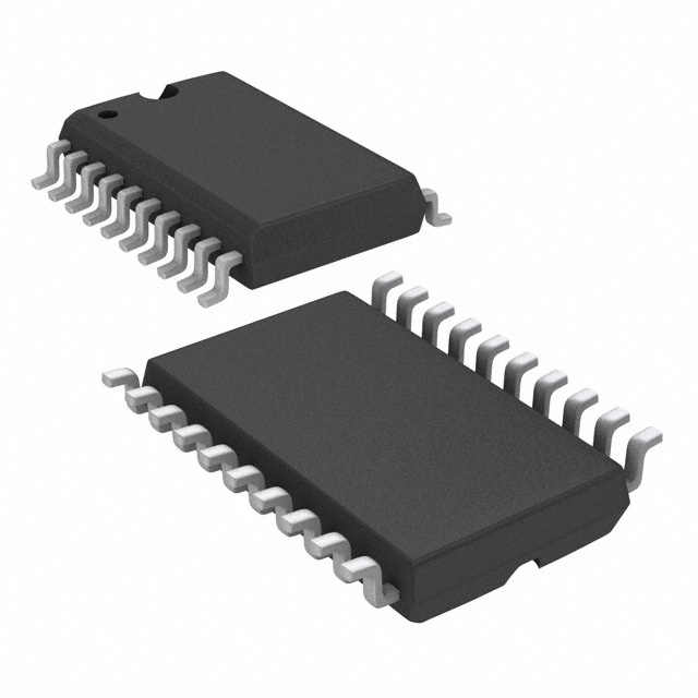
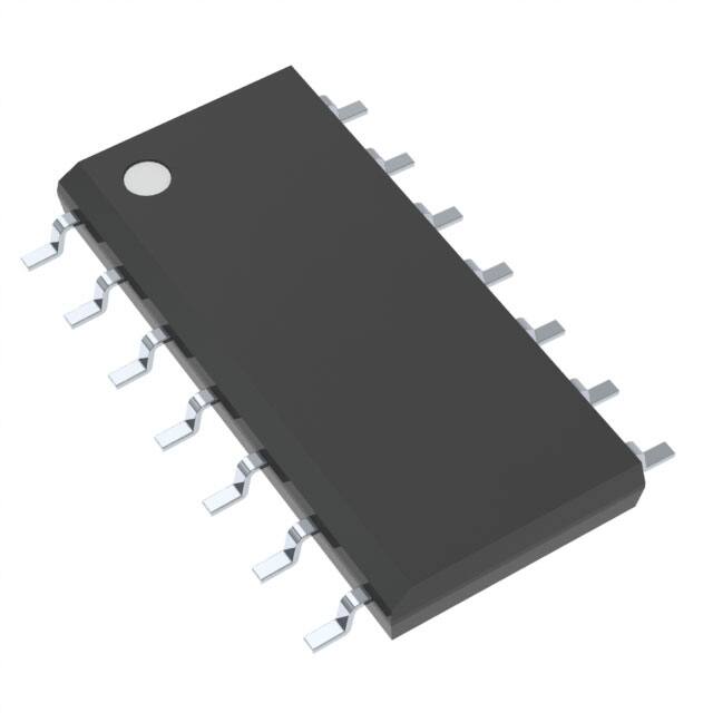
SN74LVC823ADWR
Compare
SN74LVC823ADWR
IC FF D-TYPE SNGL 9BIT 20SOIC


Compare
Price negotiable
Price update:a months ago
Available in stock:
4746


45
Serves customers in 45 countries
1000+
Worldwide Manufacturers
$140M
$140M Growth in 5 Years
50.0M+
50M Parts Shipped in 5 Years

Texas Instruments
Texas Instruments Incorporated (TI) is a global semiconductor powerhouse, crafts advanced analog ICs and embedded processors. Fueled by top-tier minds, TI's innovations drive tech's future, impacting 100,000+ clients.
View All Product from Texas Instruments


This 9-bit bus-interface flip-flop is designed for 1.65-V to 3.6-V VCC operation.
The SN74LVC823ADWR is designed specifically for driving highly capacitive or relatively low-impedance loads. It is particularly suitable for implementing wider buffer registers, I/O ports, bidirectional bus drivers with parity, and working registers.
With the clock-enable (CLKEN)\ input low, the nine D-type edge-triggered flip-flops enter data on the low-to-high transitions of the clock. Taking CLKEN\ high disables the clock buffer, latching the outputs. This device has noninverting data (D) inputs. Taking the clear (CLR)\ input low causes the nine Q outputs to go low, independently of the clock.
A buffered output-enable (OE)\ input can be used to place the nine outputs in either a normal logic state (high or low logic levels) or the high-impedance state. OE\ does not affect the internal operations of the latch. Previously stored data can be retained or new data can be entered while the outputs are in the high-impedance state.
Inputs can be driven from either 3.3-V or 5-V devices. This feature allows the use of these devices as translators in a mixed 3.3-V/5-V system environment.
This device is fully specified for partial-power-down applications using Ioff. The Ioff circuitry disables the outputs, preventing damaging current backflow through the device when it is powered down.
To ensure the high-impedance state during power up or power down, OE\ should be tied to VCC through a pullup resistor; the minimum value of the resistor is determined by the current-sinking capability of the driver.
Feature
- Operates From 1.65 V to 3.6 V
- Inputs Accept Voltages to 5.5 V
- Max tpd of 7.9 ns at 3.3 V
- Typical VOLP (Output Ground Bounce) <0.8 V at VCC = 3.3 V, TA = 25°C
- Typical VOHV (Output VOH Undershoot) >2 V at VCC = 3.3 V, TA = 25°C
- Supports Mixed-Mode Signal Operation on All Ports (5-V Input/Output Voltage With 3.3-V VCC)
- Ioff Supports Partial-Power-Down Mode Operation
- Latch-Up Performance Exceeds 250 mA Per JESD 17
- ESD Protection Exceeds JESD 22
- 2000-V Human-Body Model (A114-A)
- 200-V Machine Model (A115-A)
- 1000-V Charged-Device Model (C101)


Related Products
| Mfr Part # | Price ($) | Quantity Available | |
|---|---|---|---|
 SN74LS173ANIC FF D-TYPE SNGL 4BIT 16DIP | 0.41 |
4813
Marketplace | |
 SN74LS245NIC TXRX NON-INVERT 5.25V 20DIP | 0.28 |
5000
Marketplace | |
 SN74LS27NIC GATE NOR 3CH 3-INP 14DIP | 0.28 |
483
Marketplace |
Product Attributes
| TYPE | DESCRIPTION | Select all |
|---|---|---|
| Number of Elements | 1 | |
| Output Type | Tri-State, Non-Inverted | |
| Package / Case | 24-SOIC (0.295", 7.50mm Width) | |
| Type | D-Type | |
| Supplier Device Package | 24-SOIC | |
| Input Capacitance | 5 pF | |
| Function | Master Reset | |
| Mounting Type | Surface Mount | |
| Current - Quiescent (Iq) | 10 µA | |
| Product Status | Obsolete | |
| Operating Temperature | -40°C ~ 85°C (TA) | |
| Package | Tape & Reel (TR) | |
| Voltage - Supply | 1.65V ~ 3.6V | |
| Series | 74LVC | |
| Current - Output High, Low | 24mA, 24mA | |
| Trigger Type | Positive Edge | |
| Max Propagation Delay @ V, Max CL | 8ns @ 3.3V, 50pF | |
| Clock Frequency | 150 MHz | |
| Number of Bits per Element | 9 |
Blog


 Unveiling the Future: The Surge of Microcontrollers in 2024In the dynamic world of electronic components, microcontrollers stand out as a testament to innovation and versatility. As we edge closer to 2024, the landscape for microcontrollers and semiconductors, spearheaded by giants like STMicroelectronics, Texas Instruments, and Microchip, is set for remarkable transformation.
 Microcontrollers vs. Microprocessors: Unveiling the Core Differences for Embedded Systems EngineeringSeasoned professionals in the realm of embedded systems engineering and product development within the electronics sphere often grapple with distinguishing between microcontrollers and microprocessors. Despite their foundational role in the design and fabrication of a myriad of electronic gadgets, understanding their unique functionalities based on mere definitions can be challenging:
 A Deep Dive into the Global Ceramic Capacitors MarketJoin us in exploring the emerging subplot of environmental consciousness within the global ceramic capacitors market.
 Mastering Current Measurement with MicrocontrollersUnlock precise current measurement secrets with Microcontrollers! Conquer challenges, meet superhero solutions, and revolutionize accuracy with on-chip Analog Core Independent Peripherals (CIPs).
 What is a Rectifier Diode: A Guide to BeginnersMeet the unsung heroes of electronics—Rectifier Diodes! Explore their magic, applications, and join the behind-the-scenes adventure into gadget power.


Price negotiable
Price update:a months ago
Available in stock:
4746
Texas Instruments
Texas Instruments Incorporated (TI) is a global semiconductor powerhouse, crafts advanced analog ICs and embedded processors. Fueled by top-tier minds, TI's innovations drive tech's future, impacting 100,000+ clients.
View All Product from Texas InstrumentsBlog
- Unveiling the Future: The Surge of Microcontrollers in 2024In the dynamic world of electronic components, microcontrollers stand out as a testament to innovation and versatility. As we edge closer to 2024, the landscape for microcontrollers and semiconductors, spearheaded by giants like STMicroelectronics, Texas Instruments, and Microchip, is set for remarkable transformation.
- Microcontrollers vs. Microprocessors: Unveiling the Core Differences for Embedded Systems EngineeringSeasoned professionals in the realm of embedded systems engineering and product development within the electronics sphere often grapple with distinguishing between microcontrollers and microprocessors. Despite their foundational role in the design and fabrication of a myriad of electronic gadgets, understanding their unique functionalities based on mere definitions can be challenging:
- A Deep Dive into the Global Ceramic Capacitors MarketJoin us in exploring the emerging subplot of environmental consciousness within the global ceramic capacitors market.
- Mastering Current Measurement with MicrocontrollersUnlock precise current measurement secrets with Microcontrollers! Conquer challenges, meet superhero solutions, and revolutionize accuracy with on-chip Analog Core Independent Peripherals (CIPs).
- What is a Rectifier Diode: A Guide to BeginnersMeet the unsung heroes of electronics—Rectifier Diodes! Explore their magic, applications, and join the behind-the-scenes adventure into gadget power.
Popular Manufacturers
View all manufactures More


Popular Parts Number
More Electronic Parts More
SN74HCT574PWR
IC FF D-TYPE SNGL 8BIT 20TSSOP
SN74HCS74QDRQ1
IC FF D-TYPE DUAL 1BIT 14SOIC

SN74HCS72QDRQ1
IC FF D-TYPE DUAL 2BIT 14SOIC

CD74ACT109E
IC FF JK TYPE DUAL 1BIT 16DIP
SN74HCT273PWR
IC FF D-TYPE SNGL 8BIT 20TSSOP
SN74HC574NSR
IC FF D-TYPE SNGL 8BIT 20SO

SN74HC273QDWRG4Q1
IC FF D-TYPE SNGL 8BIT 20SOIC
SN74LVC74ADT
IC FF D-TYPE DUAL 1BIT 14SOIC
SN74F174AD
IC FF D-TYPE SNGL 6BIT 16SOIC
74AC11175DWR
D FLIP-FLOP, AC SERIES