


$0.27
Price update:a months ago
Available in stock:
38895


45
Serves customers in 45 countries
1000+
Worldwide Manufacturers
$140M
$140M Growth in 5 Years
50.0M+
50M Parts Shipped in 5 Years

Texas Instruments
Texas Instruments Incorporated (TI) is a global semiconductor powerhouse, crafts advanced analog ICs and embedded processors. Fueled by top-tier minds, TI's innovations drive tech's future, impacting 100,000+ clients.
View All Product from Texas Instruments


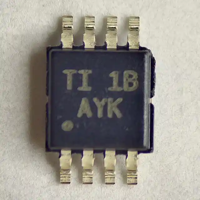
The TCA9517is abidirectional buffer with level shifting capabilities for I2C and SMBussystems. It provides bidirectional voltage-level translation (up-translation/down-translation)between low voltages (down to 0.9 V) and higher voltages (2.7 V to 5.5 V) in mixed-modeapplications. This device enables I2C and SMBus systems to be extendedwithout degradation of performance, even during level shifting.
The TCA9517buffersboth the serial data (SDA) and the serial clock (SCL) signals on the I2Cbus, thus allowing two buses of up to 400-pF bus capacitance to be connected in anI2C application.
The TCA9517has twotypes of drivers: A-side drivers and B-side drivers. All inputs and I/Os are over-voltage tolerantto 5.5 V, even when the device is unpowered (VCCB and/orVCCA = 0V).
The type of buffer design on the B-sideprevents it from being used in series with devices which use static voltage offset. This is becausethese devices do not recognize buffered low signals as a valid low and do not propagate it as abuffered low again.
The B-side drivers operate from 2.7V to 5.5V. The output low level for this internalbuffer is approximately 0.5V, but the input voltage must be 70mV or more below the output lowlevel when the output internally is driven low. The higher-voltage low signal is called a bufferedlow. When the B-side I/O is driven low internally, the low is not recognized as a low by the input.This feature prevents a lockup condition from occurring when the input low condition is released.
The A-side drivers operate from 0.9V to 5.5V and drive more current. They do notrequire the buffered low feature (or the static offset voltage). This means that a low signal onthe B-side translates to a nearly 0 V low on the A-side, which accommodates smaller voltage swingsof lower-voltage logic. The output pulldown on the A-side drives a hard low, and the input level isset at 0.3 ×VCCA to accommodate the need for a lower low level in systemswhere the low-voltage-side supply voltage is as low as 0.9V.
The A-side of two or more TCA9517DGKR s can be connected together, allowing many topographies (SeeFigure 8 andFigure 9 ), with the A-side as the common bus.Also, the A-side can be connected directly to any other buffer with static- or dynamic-offsetvoltage. Multiple TCA9517DGKR s canbe connected in series, A-side to B-side, with no buildup in offset voltage and with onlytime-of-flight delays to consider. The TCA9517cannot be connected B-side to B-side, because of the buffered lowvoltage from the B-side. The B-side cannot be connected to a device with rise time accelerators.
VCCA is only used to provide the 0.3 × VCCA reference to theA-side input comparators and for the power-good-detect circuit. The TCA9517logic and all I/Os arepowered by the VCCB pin.
As with the standard I2C system, pullup resistors are requiredto provide the logic-high levels on the buffered bus. The TCA9517DGKR has standard open-drain configuration of theI2C bus. The size of these pullup resistors depends on the system, buteach side of the repeater must have a pullup resistor. The device is designed to work with Standardmode and Fast mode I2C devices in addition to SMBus devices. Standardmode I2C devices only specify 3mA in a genericI2C system, where Standard mode devices and multiple masters arepossible. Under certain conditions, higher termination currents can be used.
Feature
- Two-Channel Bidirectional Buffer
- I2C Bus and SMBus Compatible
- Operating Supply Voltage Range of 0.9Vto5.5V on A-side
- Operating Supply Voltage Range of 2.7Vto5.5V on B-side
- Voltage-Level Translation From 0.9V - 5.5V to 2.7V-5.5V
- Footprint and Functional Replacement for PCA9515B
- Active-High Repeater-Enable Input
- Open-Drain I2C I/O
- 5.5-V Tolerant I2C and Enable Input Support Mixed-ModeSignal Operation
- Accommodates Standard Mode and Fast Mode I2C Devices andMultiple Masters
- High-Impedance I2C Pins When Powered-Off
- Latch-Up Performance Exceeds 100 mA Per JESD 78, Class II
- ESD Protection Exceeds JESD 22
- 5500 V Human-Body Model (A114-A)
- 200 V Machine Model (A115-A)
- 1000 V Charged-Device Model (C101)
All trademarks are the property of their respective owners.


Product Attributes
| TYPE | DESCRIPTION | Select all |
|---|---|---|
| Series | TCA | |
| Package | Tape & Reel (TR) | |
| Product Status | Active | |
| Translator Type | Voltage Level | |
| Channel Type | Bidirectional | |
| Number of Circuits | 1 | |
| Channels per Circuit | 2 | |
| Voltage - VCCA | 0.9 V ~ 5.5 V | |
| Voltage - VCCB | 2.7 V ~ 5.5 V | |
| Output Type | Open Drain | |
| Operating Temperature | -40°C ~ 85°C (TA) | |
| Mounting Type | Surface Mount | |
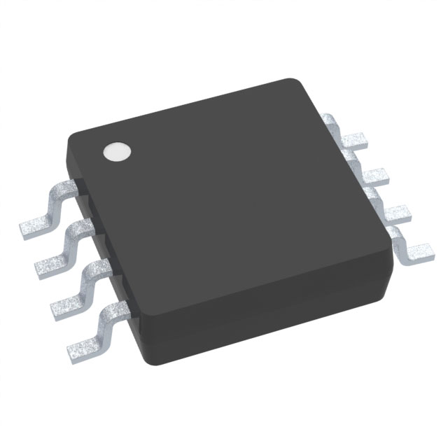
| Package / Case | 8-TSSOP, 8-MSOP (0.118", 3.00mm Width) | |
| Supplier Device Package | 8-VSSOP |
Blog


 Unveiling the Future: The Surge of Microcontrollers in 2024In the dynamic world of electronic components, microcontrollers stand out as a testament to innovation and versatility. As we edge closer to 2024, the landscape for microcontrollers and semiconductors, spearheaded by giants like STMicroelectronics, Texas Instruments, and Microchip, is set for remarkable transformation.
 Microcontrollers vs. Microprocessors: Unveiling the Core Differences for Embedded Systems EngineeringSeasoned professionals in the realm of embedded systems engineering and product development within the electronics sphere often grapple with distinguishing between microcontrollers and microprocessors. Despite their foundational role in the design and fabrication of a myriad of electronic gadgets, understanding their unique functionalities based on mere definitions can be challenging:
 A Deep Dive into the Global Ceramic Capacitors MarketJoin us in exploring the emerging subplot of environmental consciousness within the global ceramic capacitors market.
 Mastering Current Measurement with MicrocontrollersUnlock precise current measurement secrets with Microcontrollers! Conquer challenges, meet superhero solutions, and revolutionize accuracy with on-chip Analog Core Independent Peripherals (CIPs).
 What is a Rectifier Diode: A Guide to BeginnersMeet the unsung heroes of electronics—Rectifier Diodes! Explore their magic, applications, and join the behind-the-scenes adventure into gadget power.


$0.27
Price update:a months ago
Available in stock:
38895
Texas Instruments
Texas Instruments Incorporated (TI) is a global semiconductor powerhouse, crafts advanced analog ICs and embedded processors. Fueled by top-tier minds, TI's innovations drive tech's future, impacting 100,000+ clients.
View All Product from Texas InstrumentsBlog
- Unveiling the Future: The Surge of Microcontrollers in 2024In the dynamic world of electronic components, microcontrollers stand out as a testament to innovation and versatility. As we edge closer to 2024, the landscape for microcontrollers and semiconductors, spearheaded by giants like STMicroelectronics, Texas Instruments, and Microchip, is set for remarkable transformation.
- Microcontrollers vs. Microprocessors: Unveiling the Core Differences for Embedded Systems EngineeringSeasoned professionals in the realm of embedded systems engineering and product development within the electronics sphere often grapple with distinguishing between microcontrollers and microprocessors. Despite their foundational role in the design and fabrication of a myriad of electronic gadgets, understanding their unique functionalities based on mere definitions can be challenging:
- A Deep Dive into the Global Ceramic Capacitors MarketJoin us in exploring the emerging subplot of environmental consciousness within the global ceramic capacitors market.
- Mastering Current Measurement with MicrocontrollersUnlock precise current measurement secrets with Microcontrollers! Conquer challenges, meet superhero solutions, and revolutionize accuracy with on-chip Analog Core Independent Peripherals (CIPs).
- What is a Rectifier Diode: A Guide to BeginnersMeet the unsung heroes of electronics—Rectifier Diodes! Explore their magic, applications, and join the behind-the-scenes adventure into gadget power.
Popular Manufacturers
View all manufactures More


Popular Parts Number
More Electronic Parts MoreTCA9517DGKR
IC TRANSLTR BIDIRECTIONAL 8VSSOP
TCA9517DGKRQ1
IC TRANSLTR BIDIRECTIONAL 8VSSOP
SN74LVC1T45DRLR
IC TRANSLTR BIDIRECTIONAL SOT5X3

TXB0104QPWRQ1
IC TRANSLATOR BIDIR 14TSSOP
LSF0108PWR
IC TRANSLATOR BIDIR 20TSSOP
TXB0104QRUTRQ1
IC TRANSLTR BIDIRECTIONAL 12UQFN
TXS0104EYZTR
IC TRANSLATOR BIDIR 12DSBGA
SN74AXC4T774RSVR
IC TRANSLTR BIDIRECTIONAL 16UQFN
SN74AVC4T234ZWAR
IC TRANSLATOR UNIDIR 11NFBGA
TXB0106RGYR
IC TRANSLTR BIDIRECTIONAL 16VQFN