
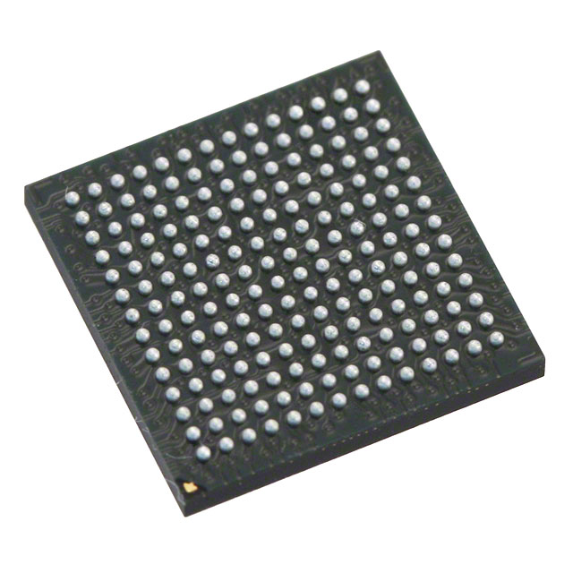
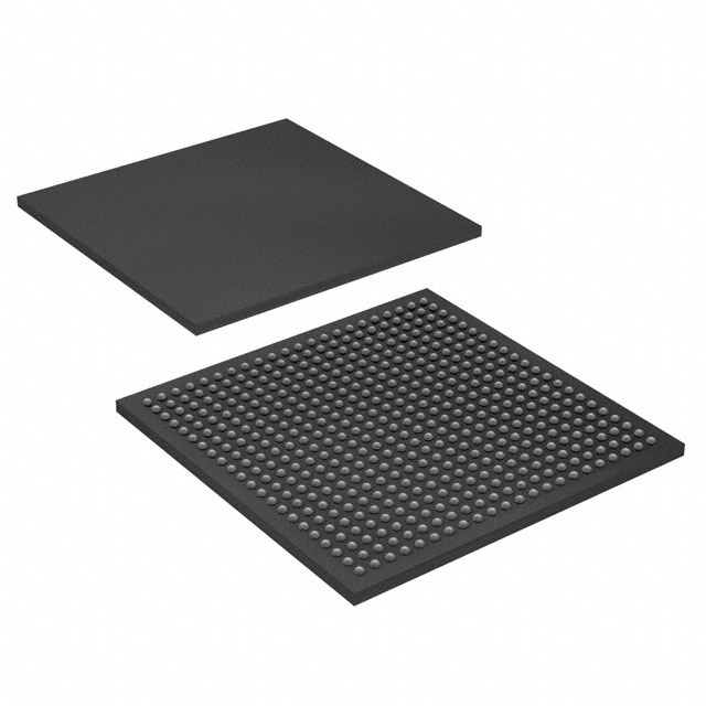
XCKU085-2FLVA1517E
Compare
XCKU085-2FLVA1517E
IC FPGA 624 I/O 1517FCBGA


Compare
$771.68
Price update:a months ago
Available in stock:
800


45
Serves customers in 45 countries
1000+
Worldwide Manufacturers
$140M
$140M Growth in 5 Years
50.0M+
50M Parts Shipped in 5 Years

Xilinx
Xilinx stands as a preeminent purveyor of All Programmable Field-Programmable Gate Arrays (FPGAs), System on Chips (SoCs), Multiprocessor System on Chips (MPSoCs), and Three-Dimensional Integrated Circuits (3D ICs). AMD stands in a distinctive position, facilitating applications that embody a dual nature of software-defined sophistication and hardware-honed optimization. This empowering of industries finds its zenith in the realms of Cloud Computing, 5G Wireless Connectivity, Embedded Vision, and the sprawling domain of Industrial Internet of Things (IIoT).
View All Product from Xilinx


_tmb.jpg)

Xilinx® UltraScale™ architecture comprises high-performance FPGA and MPSoC families that address a vast spectrum of system requirements with a focus on lowering total power consumption through numerous innovative technological advancements.
Kintex® UltraScale FPGAs: High-performance FPGAs with a focus on price/performance, using both monolithic and next-generation stacked silicon interconnect (SSI) technology. High DSP and block RAM-to-logic ratios and next-generation transceivers, combined with low-cost packaging, enable an optimum blend of capability and cost.
Kintex UltraScale+™ FPGAs: Based on the UltraScale architecture, these devices have increased performance and on-chip UltraRAM memory to reduce BOM cost, providing the ideal mix of high-performance peripherals and cost-effective system implementation. In addition, Kintex UltraScale+ FPGAs have numerous power options that deliver the optimal balance between the required system performance and the smallest power envelope.
Virtex® UltraScale FPGAs: The industry`s most capable high-performance FPGAs enabled using both monolithic and next-generation SSI technology to achieve the highest system capacity, bandwidth, and performance. Variants of the Virtex UltraScale family are optimized to address key market and application requirements through integration of various system-level functions, delivering unprecedented embedded memory and serial connectivity capabilities.
Virtex UltraScale+ FPGAs: Based on the UltraScale architecture, these devices have the highest transceiver bandwidth, highest DSP count, and highest on-chip memory available in the industry for the ultimate in system performance. In addition, Virtex UltraScale+ FPGAs also provide numerous power options that deliver the optimal balance between the required system performance and the smallest power envelope.
Zynq® UltraScale+ MPSoCs: Combine the ARM® v8-based Cortex®-A53 high-performance energy-efficient 64-bit application processor with the ARM Cortex-R5 real-time processor and the UltraScale architecture to create the industry’s first All Programmable MPSoCs. With next-generation programmable engines, security, safety, reliability, and scalability from 32 to 64 bits, the Zynq UltraScale+ MPSoCs provide unprecedented power savings, processing, programmable acceleration, I/O, and memory bandwidth ideal for applications that require heterogeneous processing.
Feature
Processing System
UltraScale+ MPSoCs are built around a feature-rich quad-core ARM Cortex-A53 and dual-core ARM Cortex-R5 processing system (PS). In addition to the 32-bit/64-bit application processing unit (APU) and 32-bit real-time processing unit (RPU), the PS contains a dedicated ARM Mali™-400 MP2 graphics processing unit (GPU).
I/O, Transceiver, PCIe, 100G Ethernet, and 150G Interlaken
Data is transported on and off chip through a combination of the high-performance parallel SelectIO™ interface and high-speed serial transceiver connectivity. I/O blocks provide support for cutting-edge memory interface and network protocols through flexible I/O standard and voltage support. The serial transceivers in the UltraScale architecture-based devices transfer data up to 32.75Gb/s, enabling 25G+ backplane designs with dramatically lower power per bit than previous generation transceivers. All transceivers, except the PS-GTR, support the required data rates for PCIe Gen3, and Gen4 (rev 0.5), and integrated blocks for PCIe enable UltraScale devices to support up to Gen4 x8 and Gen3 x16 Endpoint and Root Port designs. Integrated blocks for 150Gb/s Interlaken and 100Gb/s Ethernet (100G MAC/PCS) extend the capabilities of UltraScale devices, enabling simple, reliable support for Nx100G switch and bridge applications.
Clocks and Memory Interfaces
UltraScale devices contain powerful clock management circuitry, including clock synthesis, buffering, and routing components that together provide a highly capable framework to meet design requirements. The clock network allows for extremely flexible distribution of clocks to minimize the skew, power consumption, and delay associated with clock signals. The clock management technology is tightly integrated with dedicated memory interface circuitry to enable support for high-performance external memories, including DDR4. In addition to parallel memory interfaces, UltraScale devices support serial memories, such as Hybrid Memory Cube (HMC).
Routing, SSI, Logic, Storage, and Signal Processing
Configurable Logic Blocks (CLBs) containing 6-input look-up tables (LUTs) and flip-flops, DSP slices with 27x18 multipliers, 36Kb block RAMs with built-in FIFO and ECC support, and 4Kx72 UltraRAM blocks (in UltraScale+ devices) are all connected with an abundance of high-performance, low-latency interconnect. In addition to logical functions, the CLB provides shift register, multiplexer, and carry logic functionality as well as the ability to configure the LUTs as distributed memory to complement the highly capable and configurable block RAMs. The DSP slice, with its 96-bit-wide XOR functionality, 27-bit pre-adder, and 30-bit A input, performs numerous independent functions including multiply accumulate, multiply add, and pattern detect. In addition to the device interconnect, in devices using SSI technology, signals can cross between super-logic regions (SLRs) using dedicated, low-latency interface tiles. These combined routing resources enable easy support for next-generation bus data widths.
Configuration, Encryption, and System Monitoring
The configuration and encryption block performs numerous device-level functions critical to the successful operation of the FPGA or MPSoC. This high-performance configuration block enables device configuration from external media through various protocols, including PCIe, often with no requirement to use multi-function I/O pins during configuration. The configuration block also provides 256-bit AES-GCM decryption capability at the same performance as unencrypted configuration. include SEU detection and correction, partial reconfiguration support, and battery-backed RAM or eFUSE technology for AES key storage to provide additional security. The System Monitor enables the monitoring of the physical environment via on-chip temperature and supply sensors and can also monitor up to 17 external analog inputs. With UltraScale+ MPSoCs, the device is booted via the Configuration and Security Unit (CSU), which supports secure boot via the 256-bit AES-GCM and SHA/384 blocks. The cryptographic engines in the CSU can be used in the MPSoC after boot for user encryption.
Migrating Devices
UltraScale and UltraScale+ families provide footprint compatibility to enable users to migrate designs from one device or family to another. Any two packages with the same footprint identifier code are footprint compatible. For example, Kintex UltraScale devices in the A1156 packages are footprint compatible with Kintex UltraScale+ devices in the A1156 packages. Likewise, Virtex UltraScale devices in the B2104 packages are compatible with Virtex UltraScale+ devices and Kintex UltraScale devices in the B2104 packages. All valid device/package combinations are provided in the Device-Package Combinations and Maximum I/Os tables in this document. Refer to UG583, UltraScale Architecture PCB Design User Guide for more detail on migrating between UltraScale and UltraScale+ devices and packages.


Related Products
| Mfr Part # | Price ($) | Quantity Available | |
|---|---|---|---|
 XCKU035-2FBVA900IIC FPGA 468 I/O 900FCBGA | 2937.51 |
135
Marketplace | |
 XCKU035-1FBVA900CIC FPGA 468 I/O 900FCBGA | 275.60 |
3582
Marketplace | |
 XCKU060-1FFVA1517IIC FPGA 624 I/O 1517FCBGA | 344.50 |
880
Marketplace | |
 XCKU060-1FFVA1517CIC FPGA 624 I/O 1517FCBGA | 399.62 |
888
Marketplace | |
 XCKU060-2FFVA1517EIC FPGA 624 I/O 1517FCBGA | 447.85 |
198
Marketplace | |
XCKU085-1FLVA1517CIC FPGA 624 I/O 1517FCBGA | 1378.00 |
3290
Marketplace |
Product Attributes
| TYPE | DESCRIPTION | Select all |
|---|---|---|
| Voltage - Supply | 0.922V ~ 0.979V | |
| Mounting Type | Surface Mount | |
| Series | Kintex® UltraScale™ | |
| Operating Temperature | 0°C ~ 100°C (TJ) | |
| Package | Bulk | |
| Package / Case | 1517-BBGA, FCBGA | |
| Product Status | Active | |
| Supplier Device Package | 1517-FCBGA (40x40) | |
| Programmable | Not Verified | |
| Number of LABs/CLBs | 62190 | |
| Number of Logic Elements/Cells | 1088325 | |
| Total RAM Bits | 58265600 | |
| Number of I/O | 624 |
Blog


 Unveiling the Future: The Surge of Microcontrollers in 2024In the dynamic world of electronic components, microcontrollers stand out as a testament to innovation and versatility. As we edge closer to 2024, the landscape for microcontrollers and semiconductors, spearheaded by giants like STMicroelectronics, Texas Instruments, and Microchip, is set for remarkable transformation.
 Microcontrollers vs. Microprocessors: Unveiling the Core Differences for Embedded Systems EngineeringSeasoned professionals in the realm of embedded systems engineering and product development within the electronics sphere often grapple with distinguishing between microcontrollers and microprocessors. Despite their foundational role in the design and fabrication of a myriad of electronic gadgets, understanding their unique functionalities based on mere definitions can be challenging:
 A Deep Dive into the Global Ceramic Capacitors MarketJoin us in exploring the emerging subplot of environmental consciousness within the global ceramic capacitors market.
 Mastering Current Measurement with MicrocontrollersUnlock precise current measurement secrets with Microcontrollers! Conquer challenges, meet superhero solutions, and revolutionize accuracy with on-chip Analog Core Independent Peripherals (CIPs).
 What is a Rectifier Diode: A Guide to BeginnersMeet the unsung heroes of electronics—Rectifier Diodes! Explore their magic, applications, and join the behind-the-scenes adventure into gadget power.


$771.68
Price update:a months ago
Available in stock:
800
Xilinx
Xilinx stands as a preeminent purveyor of All Programmable Field-Programmable Gate Arrays (FPGAs), System on Chips (SoCs), Multiprocessor System on Chips (MPSoCs), and Three-Dimensional Integrated Circuits (3D ICs). AMD stands in a distinctive position, facilitating applications that embody a dual nature of software-defined sophistication and hardware-honed optimization. This empowering of industries finds its zenith in the realms of Cloud Computing, 5G Wireless Connectivity, Embedded Vision, and the sprawling domain of Industrial Internet of Things (IIoT).
View All Product from XilinxBlog
- Unveiling the Future: The Surge of Microcontrollers in 2024In the dynamic world of electronic components, microcontrollers stand out as a testament to innovation and versatility. As we edge closer to 2024, the landscape for microcontrollers and semiconductors, spearheaded by giants like STMicroelectronics, Texas Instruments, and Microchip, is set for remarkable transformation.
- Microcontrollers vs. Microprocessors: Unveiling the Core Differences for Embedded Systems EngineeringSeasoned professionals in the realm of embedded systems engineering and product development within the electronics sphere often grapple with distinguishing between microcontrollers and microprocessors. Despite their foundational role in the design and fabrication of a myriad of electronic gadgets, understanding their unique functionalities based on mere definitions can be challenging:
- A Deep Dive into the Global Ceramic Capacitors MarketJoin us in exploring the emerging subplot of environmental consciousness within the global ceramic capacitors market.
- Mastering Current Measurement with MicrocontrollersUnlock precise current measurement secrets with Microcontrollers! Conquer challenges, meet superhero solutions, and revolutionize accuracy with on-chip Analog Core Independent Peripherals (CIPs).
- What is a Rectifier Diode: A Guide to BeginnersMeet the unsung heroes of electronics—Rectifier Diodes! Explore their magic, applications, and join the behind-the-scenes adventure into gadget power.
Popular Manufacturers
View all manufactures More


Popular Parts Number
More Electronic Parts More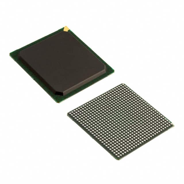
XC6SLX100-2FGG676C
IC FPGA 480 I/O 676FBGA

XC7A35T-2FGG484C
IC FPGA 250 I/O 484FBGA

XC7A50T-2FGG484I
IC FPGA 250 I/O 484FBGA
XC6SLX45T-3FGG484C
IC FPGA 296 I/O 484FBGA

XC6SLX45T-3FGG484I
IC FPGA 296 I/O 484FBGA

XC7K160T-1FBG676C
IC FPGA 400 I/O 676FCBGA
XC6SLX150-2FGG900C
IC FPGA 576 I/O 900FBGA
XC7K325T-2FFG676C
IC FPGA 400 I/O 676FCBGA
XC6SLX16-2CPG196I
IC FPGA 106 I/O 196CSBGA
XC6SLX45-3CSG484C
IC FPGA 320 I/O 484CSBGA