


$65.46
Price update:a months ago
Available in stock:
1350


45
Serves customers in 45 countries
1000+
Worldwide Manufacturers
$140M
$140M Growth in 5 Years
50.0M+
50M Parts Shipped in 5 Years

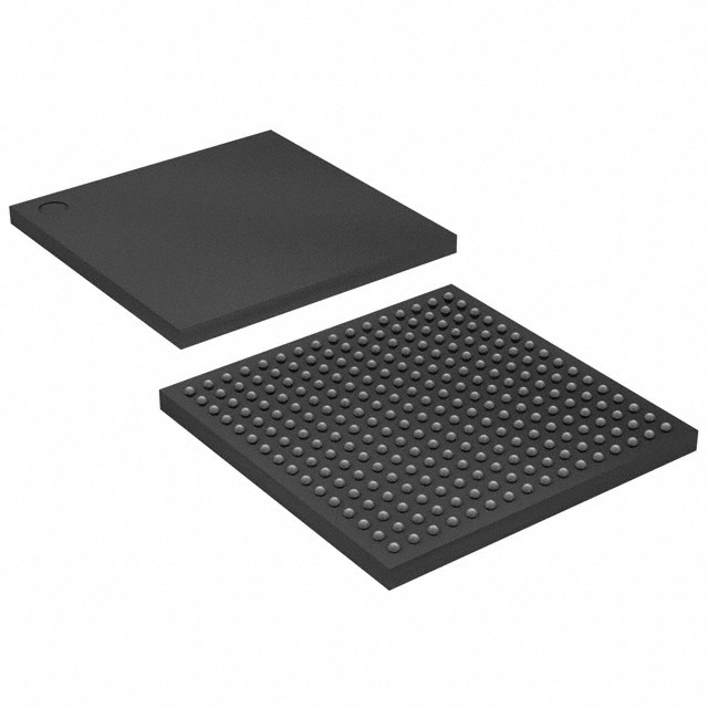
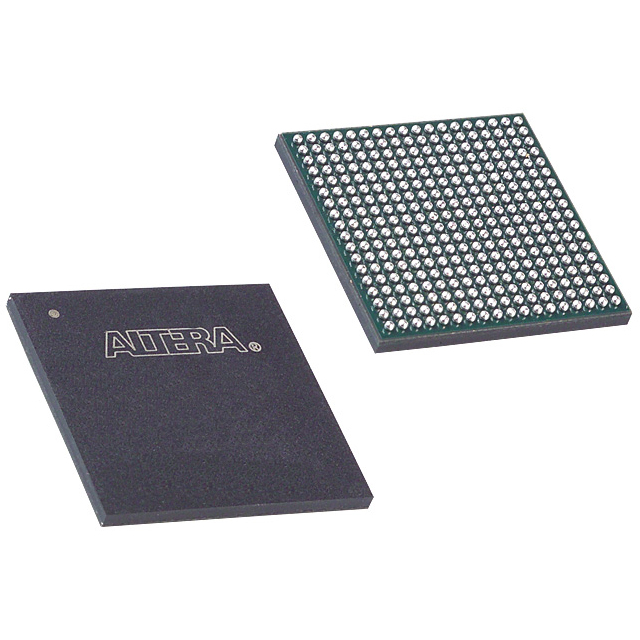
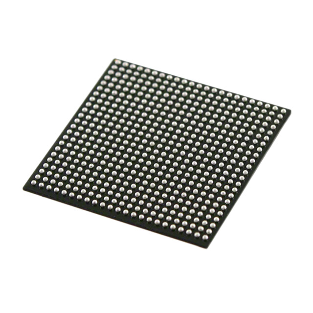
Altera
On June 1, 2015, Intel and Altera unveiled a transformative accord. Intel's acquisition of Altera concluded on December 28, 2015. This amalgamation melded Intel's cutting-edge products and manufacturing prowess with Altera's pioneering field-programmable gate array (FPGA) technology. The synergy birthed novel product classes, catering adeptly to data centers and the burgeoning Internet of Things (IoT) domain.
View All Product from Altera


_tmb.jpg)

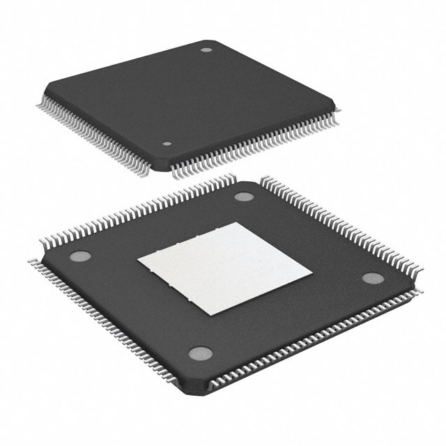
Functional
Cyclonee I devices contain a two-dimensional row-and column-basedDescrintion arhitecture toimplement custom losic. Column androw interconnects of varying speeds provide signal interconnects between logic array blocks(LABs), embedded memory blocks, and embedded multipliers.
The logic array consists of LABs, with 16 logic elements(LEs) in each LAB. An LE is a small unit of logic providing efficient implementation of user logic functions. LABs are grouped into rows and columns across the device. Cyclone II devices range in density from 4,608 to 68,416LEs.Cyclone II devices provide a global clock network and up to four phase-locked loops(PLLs). The global clock network consists of up to 16
global clock lines that drive throughout the entire device. The global clock network can provide clocks for all resources within the device, such as input/output elements(IOEs), LEs, embedded multipliers, and embedded memory blocks. The global clock lines can also be used forother high fan-out signals. Cyclone IⅡ PLLs provide general-purpose clocking with clock synthesis and phase shifting as well as external outputs for high-speed differential I/O support.
M4K memory blocks are true dual-port memory blocks with 4K bits of memory plus parity (4,608 bits). These blocks provide dedicated true dual-port, simple dual-port, or single-port memory up to 36-bits wide at up to 260 MHz. These blocks are arranged in columns across the device in between certain LABs. Cyclone II devices offer between 119 to1,152 Kbits of embedded memory.
Each embedded multiplier block can implement up to either two9×9-bit multipliers, or one 18× 18-bit multiplier with up to 250-MHz performance. Embedded multipliers are arranged in columns across the device.
Each Cyclone II device I/O pin is fed by an IOE located at the ends ofLAB rows and columns around the periphery of the device.I/O pins support various single-ended and differential I/O standards, such as the 66-and 33-MHz,64-and 32-bit PCI standard, PCI-X, and the LVDS I/O standard at a maximum data rate of 805 megabits per second(Mbps) for inputs and 640Mbps for outputs. Each IOE contains a bidirectional I/O buffer and three registers for registering input, output, and output-enable signals.
Dual-purpose DQS, DQ, and DM pins along with delay chains(used tophase-align double data rate(DDR) signals) provide interface support for external memory devices such as DDR, DDR2, and single data rate(SDR)
SDRAM, and QDRII SRAM devices at up to 167 MHz.
Figure 2-1 shows a diagram of the Cyclone lⅡ EP2C20 device.
Feature
The Cyclone II device family offers the following features:
■ High-density architecture with 4,608 to 68,416 LEs
● M4K embedded memory blocks
● Up to 1.1 Mbits of RAM available without reducing available logic
● 4,096 memory bits per block (4,608 bits per block including 512 parity bits)
● Variable port configurations of ×1, ×2, ×4, ×8, ×9, ×16, ×18, ×32, and ×36
● True dual-port (one read and one write, two reads, or two writes) operation for ×1, ×2, ×4, ×8, ×9, ×16, and ×18 modes
● Byte enables for data input masking during writes
● Up to 260-MHz operation
■ Embedded multipliers
● Up to 150 18- × 18-bit multipliers are each configurable as two independent 9- × 9-bit multipliers with up to 250-MHz performance
● Optional input and output registers


Related Products
| Mfr Part # | Price ($) | Quantity Available | |
|---|---|---|---|
 EP2C50F484C6IC FPGA 294 I/O 484FBGA | 135.73 |
2108
Marketplace | |
 EP2C35F672I8IC FPGA 475 I/O 672FBGA | 106.80 |
16
Marketplace | |
EP2C50F484C6NIC FPGA 294 I/O 484FBGA | 413.40 |
1350
Marketplace | |
 EP2C35F672I8NIC FPGA 475 I/O 672FBGA | 93.70 |
899
Marketplace |
Product Attributes
| TYPE | DESCRIPTION | Select all |
|---|---|---|
| Voltage - Supply | 1.15V ~ 1.25V | |
| Mounting Type | Surface Mount | |
| Series | Cyclone® II | |
| Operating Temperature | 0°C ~ 85°C (TJ) | |
| Package | Tray | |
| Package / Case | 484-BGA | |
| Product Status | Active | |
| Supplier Device Package | 484-FBGA (23x23) | |
| Programmable | Not Verified | |
| Number of LABs/CLBs | 3158 | |
| Number of Logic Elements/Cells | 50528 | |
| Total RAM Bits | 594432 | |
| Number of I/O | 294 |
Blog


 Unveiling the Future: The Surge of Microcontrollers in 2024In the dynamic world of electronic components, microcontrollers stand out as a testament to innovation and versatility. As we edge closer to 2024, the landscape for microcontrollers and semiconductors, spearheaded by giants like STMicroelectronics, Texas Instruments, and Microchip, is set for remarkable transformation.
 Microcontrollers vs. Microprocessors: Unveiling the Core Differences for Embedded Systems EngineeringSeasoned professionals in the realm of embedded systems engineering and product development within the electronics sphere often grapple with distinguishing between microcontrollers and microprocessors. Despite their foundational role in the design and fabrication of a myriad of electronic gadgets, understanding their unique functionalities based on mere definitions can be challenging:
 A Deep Dive into the Global Ceramic Capacitors MarketJoin us in exploring the emerging subplot of environmental consciousness within the global ceramic capacitors market.
 Mastering Current Measurement with MicrocontrollersUnlock precise current measurement secrets with Microcontrollers! Conquer challenges, meet superhero solutions, and revolutionize accuracy with on-chip Analog Core Independent Peripherals (CIPs).
 What is a Rectifier Diode: A Guide to BeginnersMeet the unsung heroes of electronics—Rectifier Diodes! Explore their magic, applications, and join the behind-the-scenes adventure into gadget power.


$65.46
Price update:a months ago
Available in stock:
1350
Altera
On June 1, 2015, Intel and Altera unveiled a transformative accord. Intel's acquisition of Altera concluded on December 28, 2015. This amalgamation melded Intel's cutting-edge products and manufacturing prowess with Altera's pioneering field-programmable gate array (FPGA) technology. The synergy birthed novel product classes, catering adeptly to data centers and the burgeoning Internet of Things (IoT) domain.
View All Product from AlteraBlog
- Unveiling the Future: The Surge of Microcontrollers in 2024In the dynamic world of electronic components, microcontrollers stand out as a testament to innovation and versatility. As we edge closer to 2024, the landscape for microcontrollers and semiconductors, spearheaded by giants like STMicroelectronics, Texas Instruments, and Microchip, is set for remarkable transformation.
- Microcontrollers vs. Microprocessors: Unveiling the Core Differences for Embedded Systems EngineeringSeasoned professionals in the realm of embedded systems engineering and product development within the electronics sphere often grapple with distinguishing between microcontrollers and microprocessors. Despite their foundational role in the design and fabrication of a myriad of electronic gadgets, understanding their unique functionalities based on mere definitions can be challenging:
- A Deep Dive into the Global Ceramic Capacitors MarketJoin us in exploring the emerging subplot of environmental consciousness within the global ceramic capacitors market.
- Mastering Current Measurement with MicrocontrollersUnlock precise current measurement secrets with Microcontrollers! Conquer challenges, meet superhero solutions, and revolutionize accuracy with on-chip Analog Core Independent Peripherals (CIPs).
- What is a Rectifier Diode: A Guide to BeginnersMeet the unsung heroes of electronics—Rectifier Diodes! Explore their magic, applications, and join the behind-the-scenes adventure into gadget power.
Popular Manufacturers
View all manufactures More


Popular Parts Number
More Electronic Parts MoreEP2C50F484C8N
IC FPGA 294 I/O 484FBGA
EP4CE6U14I7N
IC FPGA 179 I/O 256UBGA
5CGXFC3B7U15C8N
IC FPGA 144 I/O 324UBGA
EP4CGX30CF19C7N
IC FPGA 150 I/O 324FBGA
5CGXFC7C6F23C7N
IC FPGA 240 I/O 484FBGA
EP4CE6F17C8
IC FPGA 179 I/O 256FBGA
EP3C5E144C8
IC FPGA 94 I/O 144EQFP
EP2C5AF256I8N
IC FPGA 158 I/O 256FBGA
EP2C15AF484C6NES
IC FPGA 315 I/O 484FBGA

EP4CE30F23C8LN
IC FPGA 328 I/O 484FBGA