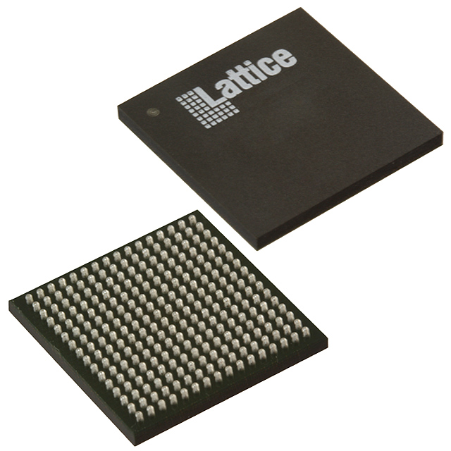
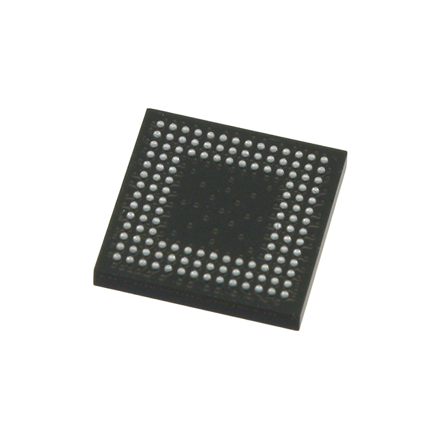
LCMXO3D-9400HC-6BG256I
Compare
LCMXO3D-9400HC-6BG256I
IC FPGA 206 I/O 256CABGA


Compare
$31.85
Price update:a months ago
Available in stock:
3385


45
Serves customers in 45 countries
1000+
Worldwide Manufacturers
$140M
$140M Growth in 5 Years
50.0M+
50M Parts Shipped in 5 Years

Lattice Semiconductor Corporation
Lattice Semiconductor leads in low-power programmability, solving complex challenges across networks, from Edge to Cloud. With a foothold in communication, computing, industry, autos, and consumers, they nurture lasting relationships, offering world-class support for unfettered innovation, crafting a secure, connected world.
View All Product from Lattice Semiconductor Corporation


The MachXO3D™ device family is the next generation of Lattice Semiconductor Low Density PLDs including enhanced security features and on-chip dual boot flash. The enhanced security features include Advanced Encryption Standard (AES) AES-128/256, Secure Hash Algorithm (SHA) SHA-256, Elliptic Curve Digital Signature Algorithm (ECDSA), Elliptic Curve Integrated Encryption Scheme (ECIES), Hash Message Authentication Code (HMAC) HMAC-SHA256, Public Key Cryptography, and Unique Secure ID. The MachXO3D family is a Root-of-Trust hardware solution that can easily scale to protect the whole system with its enhanced bitstream security and user mode functions. MachXO3D device provides breakthrough I/O density with high number of options for I/O programmability. The device I/O features the support for latest industry standard I/O, including programmable slew-rate enhancements and I3C support.
The MachXO3D family of low power, instant-on, Flash based PLDs have two devices with densities of 4300 and 9400 Look-Up Tables (LUTs). MachXO3D devices include on-chip dual boot configuration flash as well as multi-sectored User Flash Memory (UFM). In addition to LUT-based programmable logic, these devices feature Embedded Block RAM (EBR), Distributed RAM, Phase Locked Loops (PLLs), pre-engineered source synchronous I/O support, advanced configuration support including on-chip dual-boot capability and hardened versions of commonly used functions such as SPI controller, I2C controller, and timer/counter.
The MachXO3D devices are designed on a 65-nm non-volatile low power process. The device architecture has several features such as programmable low swing differential I/O and the ability to turn off I/O banks, on-chip PLLs and oscillators dynamically. These features help manage static and dynamic power consumption resulting in low power for all members of the family.
The MachXO3D devices are available in two performance levels: ultra low power (ZC) and high performance (HC). The ultra low power devices are offered in two speed grades: –2 and –3, with –3 being the fastest. Similarly, the high-performance devices are offered in two speed grades: –5 and –6, with –6 being the fastest. ZC/HC devices have an internal linear voltage regulator, which supports external VCC supply voltages of 3.3 V or 2.5 V. With the exception of power/performance profiles, the two types of devices, ZC and HC, are pin compatible with each other.
The MachXO3D PLDs are available in a broad range of advanced halogen-free packages ranging from the space saving 10 x 10 mm QFN to the 19 x 19 mm caBGA. MachXO3D devices support density migration within the same package.
The MachXO3D devices offer enhanced I/O features such as drive strength control, finer slew rate control, I3C compatibility, bus-keeper latches, pull-up resistors, pull-down resistors, open drain outputs, and hot socketing. Pull-up, pull-down, and bus-keeper features are controllable on a per-pin basis.
A user-programmable internal oscillator is included in MachXO3D devices. The clock output from this oscillator may be divided by the timer or counter for use as clock input in functions such as LED control, key-board scanner, and similar state machines.
The MachXO3D devices also provide flexible, reliable, and secure configuration from on-chip Flash with the encryption and authentication options. These devices can also configure themselves from external SPI Flash or be configured by an external master through the JTAG test access port or through the SPI/I2C port. Additionally, MachXO3D devices support on-chip dual-boot capability to reduce the system cost and remote field upgrade TransFR capability.
Lattice Semiconductor provides a variety of design tools that allow complex designs to be efficiently implemented using the MachXO3D family of devices. Popular logic synthesis tools provide synthesis library support for MachXO3D devices. Lattice design tools use the synthesis tool output along with the user-specified preferences and constraints to place and route the design in the MachXO3D device. These tools extract the timing from the routing and back-annotate it into the design for timing verification.
Lattice Semiconductor provides many pre-engineered Intellectual Property (IP) LatticeCORETM modules, including a number of reference designs licensed free of charge, optimized for the MachXO3D PLD family. By using these configurable soft core IP cores as standardized blocks, you are free to concentrate on the unique aspects of their design, increasing their productivity.
Feature
1.1.1. Solutions
Best-In-Class control PLD with advanced security functions, provide secure/authenticated boot and root of trust function
Optimized footprint, logic density, I/O count, I/O performance devices for I/O management and logic applications
High I/O logic, high I/O devices for I/O expansion applications
1.1.2. Flexible Architecture
Logic Density ranging from 4.3K to 9.4K LUT4
High I/O to LUT ratio with up to 383 I/O pins
1.1.3. Dedicated Embedded Security Block
Advanced Encryption Standard (AES): AES-128/256 Encryption/Decryption
Secure Hash Algorithm (SHA): SHA-256
Elliptic Curve Digital Signature Algorithm (ECDSA): ECDSA-based authentication
Hash Message Authentication Code (HMAC): HMAC-SHA256
Elliptic Curve Integrated Encryption Scheme (ECIES): ECIES Encryption and Decryption
True Random Number Generator (TRNG)
Key Management using Elliptic Curve DiffieHellman (ECDH) Public Key Cryptography
Unique Secure ID
Guard against malicious attacks
Interface for user logic via WISHBONE and High Speed Port (HSP)
Federal Information Processing Standard (FIPS) supported Security Protocols
1.1.4. Pre-Engineered Source Synchronous I/O
DDR registers in I/O cells
Dedicated gearing logic
7:1 Gearing for Display I/O
Generic DDR, DDRx2, DDRx4
1.1.5. High Performance, Flexible I/O Buffer
Programmable sysI/OTM buffer supports wide range of interfaces:
LVCMOS 3.3/2.5/1.8/1.5/1.2
LVTTL
LVDS, Bus-LVDS, MLVDS, LVPECL
MIPI D-PHY Emulated
Schmitt trigger inputs, up to 0.5 V hysteresis
Ideal for I/O bridging applications
I3C compatible on selective I/O
Slew rate control as Slow/Fast
I/O support hot socketing
On-chip differential termination
Programmable pull-up or pull-down mode
1.1.6. Flexible On-Chip Clocking
Eight primary clocks
Up to two edge clocks for high-speed I/O interfaces (top and bottom sides only)
Two analog PLLs per device with fractional-n frequency synthesis
Wide input frequency range (7 MHz to 400 MHz).
1.1.7. Non-volatile, Reconfigurable
Instant-on
Powers up in microseconds
On-chip dual boot
Multi-sectored UFM for customer data storage
Single-chip, secure solution
Programmable through JTAG, SPI or I2C
Reconfigurable Flash
Supports background programming of non-volatile memory
1.1.5. High Performance, Flexible I/O Buffer
Programmable sysI/OTM buffer supports wide range of interfaces:
LVCMOS 3.3/2.5/1.8/1.5/1.2
LVTTL LVDS, Bus-LVDS, MLVDS, LVPECL
MIPI D-PHY Emulated
Schmitt trigger inputs, up to 0.5 V hysteresis
Ideal for I/O bridging applications
I3C compatible on selective I/O
Slew rate control as Slow/Fast
I/O support hot socketing
On-chip differential termination
Programmable pull-up or pull-down mode
1.1.6. Flexible On-Chip Clocking
Eight primary clocks
Up to two edge clocks for high-speed I/O interfaces (top and bottom sides only)
Two analog PLLs per device with fractional-n frequency synthesis
Wide input frequency range (7 MHz to 400 MHz).
1.1.7. Non-volatile, Reconfigurable
Instant-on
Powers up in microseconds
On-chip dual boot
Multi-sectored UFM for customer data storage
Single-chip, secure solution
Programmable through JTAG, SPI or I2C
Reconfigurable Flash
Supports background programming of non-volatile memory
1.1.10. Advanced Packaging
0.5 mm pitch: 4.3K to 9.4K densities with up to 58 I/O in QFN packages
0.8 mm pitch: 4.3K to 9.4K densities with up to 383 I/O in BGA packages
Pin-compatible with MachXO3LF product family of devices
Applications
Secure boot and Root of Trust
Consumer Electronics
Compute and Storage
Wireless Communications
Industrial Control Systems
Automotive System


Related Products
| Mfr Part # | Price ($) | Quantity Available | |
|---|---|---|---|
 XCVU19P-2FSVA3824EIC FPGA 1976 I/O 3824FCBGA | 23426.00 |
780
Marketplace | |
 RT5797ALGQWIC REG BUCK ADJUSTABLE 3A 8WDFN | 0.34 |
51000
Marketplace |
Product Attributes
| TYPE | DESCRIPTION | Select all |
|---|---|---|
| Series | MachXO3D | |
| Package | Tray | |
| Product Status | Active | |
| Programmable | Not Verified | |
| Number of LABs/CLBs | 1175 | |
| Number of Logic Elements/Cells | 9400 | |
| Total RAM Bits | 442368 | |
| Number of I/O | 206 | |
| Voltage - Supply | 2.375V ~ 3.465V | |
| Mounting Type | Surface Mount | |
| Operating Temperature | -40°C ~ 100°C (TJ) | |
| Package / Case | 256-LFBGA | |
| Supplier Device Package | 256-CABGA (14x14) |
Blog


 Unveiling the Future: The Surge of Microcontrollers in 2024In the dynamic world of electronic components, microcontrollers stand out as a testament to innovation and versatility. As we edge closer to 2024, the landscape for microcontrollers and semiconductors, spearheaded by giants like STMicroelectronics, Texas Instruments, and Microchip, is set for remarkable transformation.
 Microcontrollers vs. Microprocessors: Unveiling the Core Differences for Embedded Systems EngineeringSeasoned professionals in the realm of embedded systems engineering and product development within the electronics sphere often grapple with distinguishing between microcontrollers and microprocessors. Despite their foundational role in the design and fabrication of a myriad of electronic gadgets, understanding their unique functionalities based on mere definitions can be challenging:
 A Deep Dive into the Global Ceramic Capacitors MarketJoin us in exploring the emerging subplot of environmental consciousness within the global ceramic capacitors market.
 Mastering Current Measurement with MicrocontrollersUnlock precise current measurement secrets with Microcontrollers! Conquer challenges, meet superhero solutions, and revolutionize accuracy with on-chip Analog Core Independent Peripherals (CIPs).
 What is a Rectifier Diode: A Guide to BeginnersMeet the unsung heroes of electronics—Rectifier Diodes! Explore their magic, applications, and join the behind-the-scenes adventure into gadget power.


$31.85
Price update:a months ago
Available in stock:
3385
Lattice Semiconductor Corporation
Lattice Semiconductor leads in low-power programmability, solving complex challenges across networks, from Edge to Cloud. With a foothold in communication, computing, industry, autos, and consumers, they nurture lasting relationships, offering world-class support for unfettered innovation, crafting a secure, connected world.
View All Product from Lattice Semiconductor CorporationBlog
- Unveiling the Future: The Surge of Microcontrollers in 2024In the dynamic world of electronic components, microcontrollers stand out as a testament to innovation and versatility. As we edge closer to 2024, the landscape for microcontrollers and semiconductors, spearheaded by giants like STMicroelectronics, Texas Instruments, and Microchip, is set for remarkable transformation.
- Microcontrollers vs. Microprocessors: Unveiling the Core Differences for Embedded Systems EngineeringSeasoned professionals in the realm of embedded systems engineering and product development within the electronics sphere often grapple with distinguishing between microcontrollers and microprocessors. Despite their foundational role in the design and fabrication of a myriad of electronic gadgets, understanding their unique functionalities based on mere definitions can be challenging:
- A Deep Dive into the Global Ceramic Capacitors MarketJoin us in exploring the emerging subplot of environmental consciousness within the global ceramic capacitors market.
- Mastering Current Measurement with MicrocontrollersUnlock precise current measurement secrets with Microcontrollers! Conquer challenges, meet superhero solutions, and revolutionize accuracy with on-chip Analog Core Independent Peripherals (CIPs).
- What is a Rectifier Diode: A Guide to BeginnersMeet the unsung heroes of electronics—Rectifier Diodes! Explore their magic, applications, and join the behind-the-scenes adventure into gadget power.
Popular Manufacturers
View all manufactures More


Popular Parts Number
More Electronic Parts MoreLCMXO3D-9400HC-6BG256I
IC FPGA 206 I/O 256CABGA
LCMXO1200C-4TN100C
IC FPGA 73 I/O 100TQFP
LFXP2-5E-5QN208C
IC FPGA 146 I/O 208QFP
LFE2M20E-5FN484I
IC FPGA 304 I/O 484FBGA
LCMXO2-1200HC-6MG132C
IC FPGA 104 I/O 132CSBGA
LIFCL-40-7MG121C
IC FPGA 72 I/O 121CSFBGA
LFE2M20E-6FN256C
IC FPGA 140 I/O 256FBGA
ICE40HX1K-CB132
IC FPGA 95 I/O 132CSBGA
LCMXO3LF-2100E-5MG256C
IC FPGA 206 I/O 256CSFBGA
LFD2NX-17-9MG121I
IC FPGA CERTUS-NX 121BGA