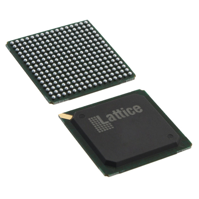
LFX125EC-03F256C
Compare
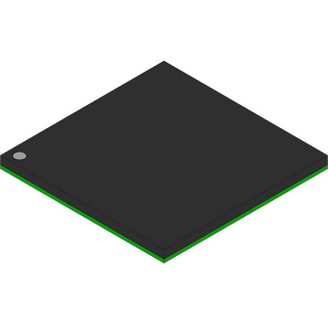
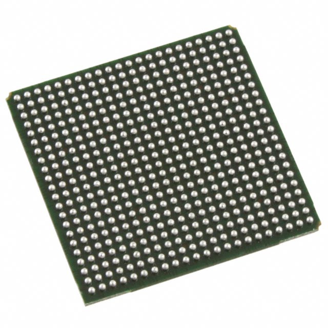
LFX125EC-03F256C
FPGA, 484 CLBS, 139000 GATES


Compare
$45.13
Price update:a months ago
Available in stock:
3


45
Serves customers in 45 countries
1000+
Worldwide Manufacturers
$140M
$140M Growth in 5 Years
50.0M+
50M Parts Shipped in 5 Years

Lattice Semiconductor Corporation
Lattice Semiconductor leads in low-power programmability, solving complex challenges across networks, from Edge to Cloud. With a foothold in communication, computing, industry, autos, and consumers, they nurture lasting relationships, offering world-class support for unfettered innovation, crafting a secure, connected world.
View All Product from Lattice Semiconductor Corporation


_tmb.jpg)


The ispXPGA family of devices provides the ideal vehicle for the creation of high-performance logic designs that are both non-volatile and infinitely re-programmable. Other FPGA solutions force a compromise, being either reprogrammable or non-volatile. This family couples this capability with a mainstream architecture containing the features required for today’s system-level design.
The ispXPGA family is available in two options. The standard device supports sysHSI capability for ultra fast serial communications while the lower-cost “E-Series” supports the same high-performance FPGA fabric without the sysHSI Block.
Electrically Erasable CMOS (E2 CMOS) memory cells provide the ispXPGA family with non-volatile capability. These allow logic to be functional microseconds after power is applied, allowing easy interfacing in many applications. This capability also means that expensive external configuration memories are not required and that designs can be secured from unauthorized read back. Internal SRAM cells allow the device to be infinitely reconfigured if desired. Both the SRAM and E2 CMOS cells can be programmed and verified through the IEEE 1532 industry standard. Additionally, the SRAM cells can be configured and read-back through the sysCONFIG™ peripheral port.
The family spans the density and I/O range required for the majority of today’s logic designs, 139K to 1.25M system gates and 160 to 496 I/O. The devices are available for operation from 1.8V, 2.5V, and 3.3V power supplies, providing easy integration into the overall system.
System-level design needs are met through the incorporation of sysMEM dual-port memory blocks, sysIO advanced I/O support, and sysCLOCK Phase Locked Loops (PLLs). High-speed serial communications are supported through multiple sysHSI blocks, which provide clock data recovery (CDR) and serialization/de-serialization (SERDES).
The ispLEVER™ design tool from Lattice allows easy implementation of designs using the ispXPGA product. Synthesis library support is available for major logic synthesis tools. The ispLEVER tool takes the output from these common synthesis packages and place and routes the design in the ispXPGA product. The tool supports floor planning and the management of other constraints within the device. The tool also provides outputs to common timing analysis tools for timing analysis.
To increase designer productivity, Lattice provides a variety of pre-designed modules referred to as IP cores for the ispXPGA product. These IP cores allow designers to concentrate on the unique portions of their design while using pre-designed blocks to implement standard functions such as bus interfaces, standard communication interfaces, and memory controllers.
Through the use of advanced technology and innovative architecture the ispXPGA FPGA devices provide designers with excellent speed performance. Although design dependent, many typical designs can run at over 150MHz. Certain designs can run at over 300MHz. Table 2 details the performance of several building blocks commonly used by logic designers.
Feature
■ Non-volatile, Infinitely Reconfigurable
• Instant-on - Powers up in microseconds via on-chip E2 CMOS® based memory
• No external configuration memory
• Excellent design security, no bit stream to intercept
• Reconfigure SRAM based logic in milliseconds
■ High Logic Density for System-level Integration
• 139K to 1.25M system gates
• 160 to 496 I/O
• 1.8V, 2.5V, and 3.3V VCC operation
• Up to 414Kb sysMEM™ embedded memory
■ High Performance Programmable Function Unit (PFU)
• Four LUT-4 per PFU supports wide and narrow functions
• Dual flip-flops per LUT-4 for extensive pipelining
• Dedicated logic for adders, multipliers, multiplexers, and counters
■ Flexible Memory Resources
• Multiple sysMEM Embedded RAM Blocks
– Single port, Dual port, and FIFO operation
• 64-bit distributed memory in each PFU
– Single port, Double port, FIFO, and Shift Register operation
■ Flexible Programming, Reconfiguration, and Testing
• Supports IEEE 1532 and 1149.1
• Microprocessor configuration interface
• Program E2 CMOS while operating from SRAM
■ Eight sysCLOCK™ Phase Locked Loops (PLLs) for Clock Management
• True PLL technology
• 10MHz to 320MHz operation
• Clock multiplication and division
• Phase adjustment
• Shift clocks in 250ps steps
■ sysIO™ for High System Performance
• High speed memory support through SSTL and HSTL
• Advanced buses supported through PCI, GTL+, LVDS, BLVDS, and LVPECL
• Standard logic supported through LVTTL, LVCMOS 3.3, 2.5 and 1.8
• 5V tolerant I/O for LVCMOS 3.3 and LVTTL interfaces
• Programmable drive strength for series termination
• Programmable bus maintenance
■ Two Options Available
• High-performance sysHSI (standard part number)
• Low-cost, no sysHSI (“E-Series”)
■ sysHSI™ Capability for Ultra Fast Serial Communications
• Up to 800Mbps performance
• Up to 20 channels per device
• Built in Clock Data Recovery (CDR) and Serialization and De-serialization (SERDES)


Product Attributes
| TYPE | DESCRIPTION | Select all |
|---|---|---|
| Number of Gates | 139000 | |
| Voltage - Supply | 2.3V ~ 3.6V | |
| Mounting Type | Surface Mount | |
| Series | ispXPGA® | |
| Operating Temperature | 0°C ~ 85°C (TJ) | |
| Package | Bulk | |
| Package / Case | 256-BGA | |
| Product Status | Active | |
| Supplier Device Package | 256-FPBGA (17x17) | |
| Programmable | Not Verified | |
| Number of LABs/CLBs | 484 | |
| Total RAM Bits | 94208 |
Blog


 Unveiling the Future: The Surge of Microcontrollers in 2024In the dynamic world of electronic components, microcontrollers stand out as a testament to innovation and versatility. As we edge closer to 2024, the landscape for microcontrollers and semiconductors, spearheaded by giants like STMicroelectronics, Texas Instruments, and Microchip, is set for remarkable transformation.
 Microcontrollers vs. Microprocessors: Unveiling the Core Differences for Embedded Systems EngineeringSeasoned professionals in the realm of embedded systems engineering and product development within the electronics sphere often grapple with distinguishing between microcontrollers and microprocessors. Despite their foundational role in the design and fabrication of a myriad of electronic gadgets, understanding their unique functionalities based on mere definitions can be challenging:
 A Deep Dive into the Global Ceramic Capacitors MarketJoin us in exploring the emerging subplot of environmental consciousness within the global ceramic capacitors market.
 Mastering Current Measurement with MicrocontrollersUnlock precise current measurement secrets with Microcontrollers! Conquer challenges, meet superhero solutions, and revolutionize accuracy with on-chip Analog Core Independent Peripherals (CIPs).
 What is a Rectifier Diode: A Guide to BeginnersMeet the unsung heroes of electronics—Rectifier Diodes! Explore their magic, applications, and join the behind-the-scenes adventure into gadget power.


$45.13
Price update:a months ago
Available in stock:
3
Lattice Semiconductor Corporation
Lattice Semiconductor leads in low-power programmability, solving complex challenges across networks, from Edge to Cloud. With a foothold in communication, computing, industry, autos, and consumers, they nurture lasting relationships, offering world-class support for unfettered innovation, crafting a secure, connected world.
View All Product from Lattice Semiconductor CorporationBlog
- Unveiling the Future: The Surge of Microcontrollers in 2024In the dynamic world of electronic components, microcontrollers stand out as a testament to innovation and versatility. As we edge closer to 2024, the landscape for microcontrollers and semiconductors, spearheaded by giants like STMicroelectronics, Texas Instruments, and Microchip, is set for remarkable transformation.
- Microcontrollers vs. Microprocessors: Unveiling the Core Differences for Embedded Systems EngineeringSeasoned professionals in the realm of embedded systems engineering and product development within the electronics sphere often grapple with distinguishing between microcontrollers and microprocessors. Despite their foundational role in the design and fabrication of a myriad of electronic gadgets, understanding their unique functionalities based on mere definitions can be challenging:
- A Deep Dive into the Global Ceramic Capacitors MarketJoin us in exploring the emerging subplot of environmental consciousness within the global ceramic capacitors market.
- Mastering Current Measurement with MicrocontrollersUnlock precise current measurement secrets with Microcontrollers! Conquer challenges, meet superhero solutions, and revolutionize accuracy with on-chip Analog Core Independent Peripherals (CIPs).
- What is a Rectifier Diode: A Guide to BeginnersMeet the unsung heroes of electronics—Rectifier Diodes! Explore their magic, applications, and join the behind-the-scenes adventure into gadget power.
Popular Manufacturers
View all manufactures More


Popular Parts Number
More Electronic Parts MoreLFX125EC-03F256C
FPGA, 484 CLBS, 139000 GATES
LFE2M20E-5FN484I
IC FPGA 304 I/O 484FBGA
LCMXO2-1200HC-6MG132C
IC FPGA 104 I/O 132CSBGA
LIFCL-40-7MG121C
IC FPGA 72 I/O 121CSFBGA
LFE2M20E-6FN256C
IC FPGA 140 I/O 256FBGA
ICE40HX1K-CB132
IC FPGA 95 I/O 132CSBGA
LCMXO3LF-2100E-5MG256C
IC FPGA 206 I/O 256CSFBGA
LFD2NX-17-9MG121I
IC FPGA CERTUS-NX 121BGA
LIFCL-40-9MG121I
IC FPGA 72 I/O 121CSFBGA
LIFCL-17-8UWG72C
IC FPGA 40 I/O 72WLCSP