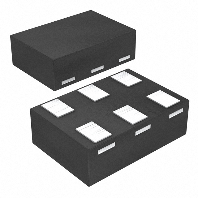
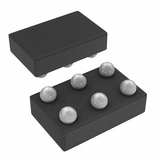
SN74AXCH1T45DRYR
Compare
SN74AXCH1T45DRYR
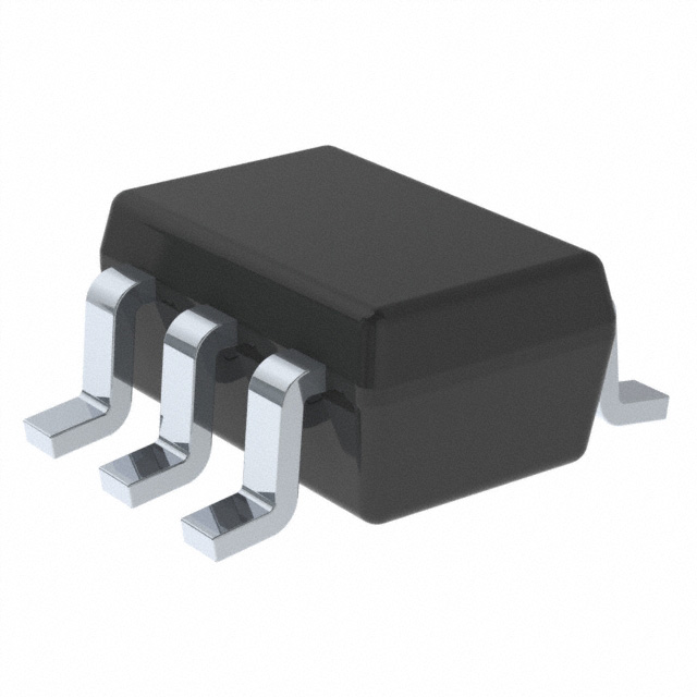
IC TRANSLTR BIDIRECTIONAL 6SON


Compare
$0.71
Price update:a months ago
Available in stock:
4183


45
Serves customers in 45 countries
1000+
Worldwide Manufacturers
$140M
$140M Growth in 5 Years
50.0M+
50M Parts Shipped in 5 Years

Texas Instruments
Texas Instruments Incorporated (TI) is a global semiconductor powerhouse, crafts advanced analog ICs and embedded processors. Fueled by top-tier minds, TI's innovations drive tech's future, impacting 100,000+ clients.
View All Product from Texas Instruments


All trademarks are the property of their respective owners.
DescriptionThe SN74AXCH1T45DBVR is a single-bit noninverting bus transceiver that uses two individuallyconfigurable power-supply rails. The device is operational with both VCCAand VCCB supplies as low as 0.65 V. The A port is designed to trackVCCA, which accepts any supply voltage from 0.65 V to 3.6 V. The B port isdesigned to track VCCB, which also accepts any supply voltage from 0.65 V to3.6 V. Additionally the SN74AXCH1T45DBVR is compatible with a single-supply system.
The DIR pin determines the direction of signal propagation. With the DIR pin configuredHIGH, translation is from Port A to Port B. With DIR configured LOW, translation is from Port B toPort A. The DIR pin is referenced to VCCA, meaning that its logic-high andlogic-low thresholds track with VCCA.
Active bus-hold circuitry holds unused or undriven inputs at a valid logic state. Use ofpullup or pulldown resistors with the bus-hold circuitry is not recommended. If a supply is presentfor VCCA or VCCB, the bus-hold circuitry alwaysremains active on the A or B inputs respectively, independent of the state of the direction controlpin.
This device is fully specified for partial-power-down applications using theIoff current. The Ioff protection circuitry ensuresthat no excessive current is drawn from or to an input, output, or combined I/O that is biased to aspecific voltage while the device is powered down.
The VCC isolation feature ensures that if eitherVCCA or VCCB is less than 100 mV, both I/O portsenter a high-impedance state by disabling their outputs.
Glitch-free power supply sequencing allows either supply rail to be powered on or off inany order while providing robust power sequencing performance.
Feature
- Fully Configurable Dual-Rail Design Allows Each Port to Operate With a Power SupplyRange from 0.65 V to 3.6 V
- Operating Temperature: –40°C to +125°C
- Glitch-Free Power Supply Sequencing
- Bus-hold on Data InputsEliminates the Need for External Pullup or Pulldown Resistors
- Maximum QuiescentCurrent (ICCA + ICCB) of 8 μA (85°C Maximum) and 14μA (125°C Maximum)
- Up to 500-Mbps Support When Translating from 1.8 to3.3V
- VCC Isolation Feature
- If Either VCC Input is Below 100 mV, All I/Os Outputsare Disabled and Become High-Impedance
- Ioff Supports Partial-Power-Down Mode Operation
- Latch-Up Performance Exceeds 100 mA Per JESD 78, Class II
- ESD Protection Exceeds JESD 22
- 8000-V Human Body Model
- 1000-V Charged-DeviceModel
All trademarks are the property of their respective owners.
DescriptionThe SN74AXCH1T45 is a single-bit noninverting bus transceiver that uses two individuallyconfigurable power-supply rails. The device is operational with both VCCAand VCCB supplies as low as 0.65 V. The A port is designed to trackVCCA, which accepts any supply voltage from 0.65 V to 3.6 V. The B port isdesigned to track VCCB, which also accepts any supply voltage from 0.65 V to3.6 V. Additionally the SN74AXCH1T45 is compatible with a single-supply system.
The DIR pin determines the direction of signal propagation. With the DIR pin configuredHIGH, translation is from Port A to Port B. With DIR configured LOW, translation is from Port B toPort A. The DIR pin is referenced to VCCA, meaning that its logic-high andlogic-low thresholds track with VCCA.
Active bus-hold circuitry holds unused or undriven inputs at a valid logic state. Use ofpullup or pulldown resistors with the bus-hold circuitry is not recommended. If a supply is presentfor VCCA or VCCB, the bus-hold circuitry alwaysremains active on the A or B inputs respectively, independent of the state of the direction controlpin.
This device is fully specified for partial-power-down applications using theIoff current. The Ioff protection circuitry ensuresthat no excessive current is drawn from or to an input, output, or combined I/O that is biased to aspecific voltage while the device is powered down.
The VCC isolation feature ensures that if eitherVCCA or VCCB is less than 100 mV, both I/O portsenter a high-impedance state by disabling their outputs.
Glitch-free power supply sequencing allows either supply rail to be powered on or off inany order while providing robust power sequencing performance.


Product Attributes
| TYPE | DESCRIPTION | Select all |
|---|---|---|
| Channel Type | Bidirectional | |
| Mounting Type | Surface Mount | |
| Translator Type | Voltage Level | |
| Product Status | Active | |
| Operating Temperature | -40°C ~ 125°C (TA) | |
| Package | Tape & Reel (TR) | |
| Data Rate | 500Mbps | |
| Output Type | Tri-State, Non-Inverted | |
| Series | 74AXCH | |
| Voltage - VCCB | 0.65 V ~ 3.6 V | |
| Voltage - VCCA | 0.65 V ~ 3.6 V | |
| Channels per Circuit | 1 | |
| Supplier Device Package | 6-SON (1.45x1) | |
| Number of Circuits | 1 | |
| Package / Case | 6-UFDFN |
Blog


 Unveiling the Future: The Surge of Microcontrollers in 2024In the dynamic world of electronic components, microcontrollers stand out as a testament to innovation and versatility. As we edge closer to 2024, the landscape for microcontrollers and semiconductors, spearheaded by giants like STMicroelectronics, Texas Instruments, and Microchip, is set for remarkable transformation.
 Microcontrollers vs. Microprocessors: Unveiling the Core Differences for Embedded Systems EngineeringSeasoned professionals in the realm of embedded systems engineering and product development within the electronics sphere often grapple with distinguishing between microcontrollers and microprocessors. Despite their foundational role in the design and fabrication of a myriad of electronic gadgets, understanding their unique functionalities based on mere definitions can be challenging:
 A Deep Dive into the Global Ceramic Capacitors MarketJoin us in exploring the emerging subplot of environmental consciousness within the global ceramic capacitors market.
 Mastering Current Measurement with MicrocontrollersUnlock precise current measurement secrets with Microcontrollers! Conquer challenges, meet superhero solutions, and revolutionize accuracy with on-chip Analog Core Independent Peripherals (CIPs).
 What is a Rectifier Diode: A Guide to BeginnersMeet the unsung heroes of electronics—Rectifier Diodes! Explore their magic, applications, and join the behind-the-scenes adventure into gadget power.


$0.71
Price update:a months ago
Available in stock:
4183
Texas Instruments
Texas Instruments Incorporated (TI) is a global semiconductor powerhouse, crafts advanced analog ICs and embedded processors. Fueled by top-tier minds, TI's innovations drive tech's future, impacting 100,000+ clients.
View All Product from Texas InstrumentsBlog
- Unveiling the Future: The Surge of Microcontrollers in 2024In the dynamic world of electronic components, microcontrollers stand out as a testament to innovation and versatility. As we edge closer to 2024, the landscape for microcontrollers and semiconductors, spearheaded by giants like STMicroelectronics, Texas Instruments, and Microchip, is set for remarkable transformation.
- Microcontrollers vs. Microprocessors: Unveiling the Core Differences for Embedded Systems EngineeringSeasoned professionals in the realm of embedded systems engineering and product development within the electronics sphere often grapple with distinguishing between microcontrollers and microprocessors. Despite their foundational role in the design and fabrication of a myriad of electronic gadgets, understanding their unique functionalities based on mere definitions can be challenging:
- A Deep Dive into the Global Ceramic Capacitors MarketJoin us in exploring the emerging subplot of environmental consciousness within the global ceramic capacitors market.
- Mastering Current Measurement with MicrocontrollersUnlock precise current measurement secrets with Microcontrollers! Conquer challenges, meet superhero solutions, and revolutionize accuracy with on-chip Analog Core Independent Peripherals (CIPs).
- What is a Rectifier Diode: A Guide to BeginnersMeet the unsung heroes of electronics—Rectifier Diodes! Explore their magic, applications, and join the behind-the-scenes adventure into gadget power.
Popular Manufacturers
View all manufactures More


Popular Parts Number
More Electronic Parts MoreSN74AXCH1T45DRYR
IC TRANSLTR BIDIRECTIONAL 6SON
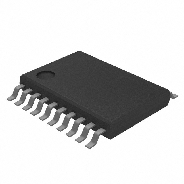
LSF0108PWR
IC TRANSLATOR BIDIR 20TSSOP
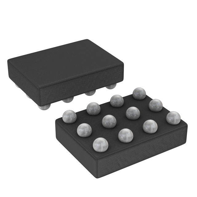
TXS0104EYZTR
IC TRANSLATOR BIDIR 12DSBGA
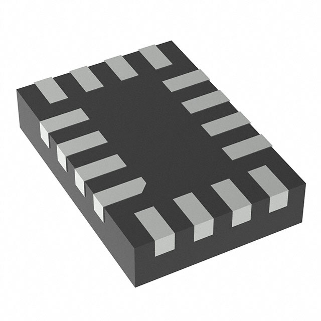
SN74AXC4T774RSVR
IC TRANSLTR BIDIRECTIONAL 16UQFN
TXB0108DQSR
IC TRANSLTR BIDIRECTIONAL 20USON
SN74LVC1T45DCKT
IC TRANSLTR BIDIRECTIONAL SC70-6
TXS0104ED
IC TRANSLTR BIDIRECTIONAL 14SOIC
SN74LVC4245ADW
IC TRANSLTR BIDIRECTIONAL 24SOIC
TXB0101YZPR
IC TRANSLTR BIDIRECTIONAL 6DSBGA
TXB0304RSVR
IC TRANSLTR BIDIRECTIONAL 16UQFN