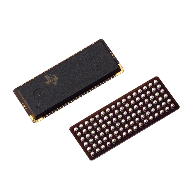
SN74SSTUB32866NMJR
Compare
SN74SSTUB32866NMJR
IC CONFIG REG BUFF 25BIT 96-BGA


Compare
$7.44
Price update:a months ago
Available in stock:
4702


45
Serves customers in 45 countries
1000+
Worldwide Manufacturers
$140M
$140M Growth in 5 Years
50.0M+
50M Parts Shipped in 5 Years

Texas Instruments
Texas Instruments Incorporated (TI) is a global semiconductor powerhouse, crafts advanced analog ICs and embedded processors. Fueled by top-tier minds, TI's innovations drive tech's future, impacting 100,000+ clients.
View All Product from Texas Instruments


This 25-bit 1:1 or 14-bit 1:2 configurable registered buffer is designed for 1.7-V to 1.9-V VCC operation. In the1:1 pinout configuration, only one device per DIMM is required to drive nine SDRAM loads. In the 1:2 pinout configuration, two devices per DIMM are required to drive 18 SDRAM loads.
All inputs are SSTL_18, except the reset (RESET) and control (Cn) inputs, which are LVCMOS. All outputs are edge-controlled circuits optimized for unterminated DIMM loads and meet SSTL_18 specifications, except the open-drain error (QERR) output.
The SN74SSTUB32866ZKER operates from a differential clock (CLK and CLK). Data are registered at the crossing of CLK going high and CLK going low.
The SN74SSTUB32866ZKER accepts a parity bit from the memory controller on the parity bit (PAR_IN) input, compares it with the data received on the DIMM-independent D-inputs (D2-D3, D5-D6, D8-D25 when C0 = 0 and C1 = 0; D2-D3, D5-D6, D8-D14 when C0 = 0 and C1 = 1; or D1-D6, D8-D13 when C0 = 1 and C1 = 1) and indicates whether a parity error has occurred on the open-drain QERR pin (active low). The convention is even parity; i.e., valid parity is defined as an even number of ones across the DIMM-independent data inputs, combined with the parity input bit. To calculate parity, all DIMM-independent data inputs must be tied to a known logic state.
When used as a single device, the C0 and C1 inputs are tied low. In this configuration, parity is checked on the PAR_IN input signal, which arrives one cycle after the input data to which it applies. Two clock cycles after the data are registered, the corresponding partial-parity-out (PPO) and QERR signals are generated.
When used in pairs, the C0 input of the first register is tied low, and the C0 input of the second register is tied high. The C1 input of both registers are tied high. Parity, which arrives one cycle after the data input to which it applies, is checked on the PAR_IN input signal of the first device. Two clock cycles after the data are registered, the corresponding PPO and QERR signals are generated on the second device. The PPO output of the first register is cascaded to the PAR_IN of the second SN74SSTUB32866. The QERR output of the first SN74SSTUB32866ZKER is left floating, and the valid error information is latched on the QERR output of the second SN74SSTUB32866.
If an error occurs and the QERR output is driven low, it stays latched low for a minimum of two clock cycles or until RESET is driven low. If two or more consecutive parity errors occur, the QERR output is driven low and latched low for a clock duration equal to the parity-error duration or until RESET is driven low. The DIMM-dependent signals (DCKE, DCS, DODT, and CSR) are not included in the parity-check computation.
The C0 input controls the pinout configuration of the 1:2 pinout from register-A configuration (when low) to register-B configuration (when high). The C1 input controls the pinout configuration from 25-bit 1:1 (when low) to 14-bit 1:2 (when high). C0 and C1 should not be switched during normal operation. They should be hard-wired to a valid low or high level to configure the register in the desired mode. In the 25-bit 1:1 pinout configuration, the A6, D6, and H6 terminals are driven low and are do-not-use (DNU) pins.
In the DDR2 RDIMM application, RESET is specified to be completely asynchronous with respect to CLK and CLK. Therefore, no timing relationship can be ensured between the two. When entering reset, the register is cleared, and the data outputs are driven low quickly, relative to the time required to disable the differential input receivers. However, when coming out of reset, the register becomes active quickly, relative to the time required to enable the differential input receivers. As long as the data inputs are low, and the clock is stable during the time from the low-to-high transition of RESET until the input receivers are fully enabled, the design of the SN74SSTUB32866ZKER ensures that the outputs remain low, thus ensuring there will be no glitches on the output.
To ensure defined outputs from the register before a stable clock has been supplied, RESET must be held in the low state during power up.
The device supports low-power standby operation. When RESET is low, the differential input receivers are disabled, and undriven (floating) data, clock, and reference voltage (VREF) inputs are allowed. In addition, when RESET is low, all registers are reset and all outputs are forced low, except QERR. The LVCMOS RESET and Cn inputs always must be held at a valid logic high or low level.
The device also supports low-power active operation by monitoring both system chip select (DCS and CSR) inputs and gates the Qn and PPO outputs from changing states when both DCS and CSR inputs are high. If either DCS or CSR input is low, the Qn and PPO outputs function normally. Also, if the internal low-power signal (LPS1) is high (one cycle after DCS and CSR go high), the device gates the QERR output from changing states. If LPS1 is low, the QERR output functions normally. The RESET input has priority over the DCS and CSR control and, when driven low, forces the Qn and PPO outputs low and forces the QERR output high. If the DCS control functionality is not desired, the CSR input can be hard-wired to ground, in which case the setup-time requirement for DCS is the same as for the other D data inputs. To control the low-power mode with DCS only, the CSR input should be pulled up to VCC through a pullup resistor.
The two VREF pins (A3 and T3) are connected together internally by approximately 150. However, it is necessary to connect only one of the two VREF pins to the external VREF power supply. An unused VREF pin should be terminated with a VREF coupling capacitor.
Feature
- Member of the Texas InstrumentsWidebus+ Family
- Pinout Optimizes DDR2 DIMM PCB Layout
- Configurable as 25-Bit 1:1 or 14-Bit 1:2 Registered Buffer
- Chip-Select Inputs Gate the Data Outputs from Changing State and Minimizes System Power Consumption
- Output Edge-Control Circuitry Minimizes Switching Noise in an Unterminated Line
- Supports SSTL_18 Data Inputs
- Differential Clock (CLK and CLK) Inputs
- Supports LVCMOS Switching Levels on the Control and RESET Inputs
- Checks Parity on DIMM-Independent Data Inputs
- Able to Cascade with a Second SN74SSTUB32866
- Supports Industrial Temperature Range (-40°C to 85°C)


Related Products
| Mfr Part # | Price ($) | Quantity Available | |
|---|---|---|---|
 SN74LS173ANIC FF D-TYPE SNGL 4BIT 16DIP | 0.41 |
4813
Marketplace | |
 SN74LS245NIC TXRX NON-INVERT 5.25V 20DIP | 0.28 |
5000
Marketplace | |
 SN74LS27NIC GATE NOR 3CH 3-INP 14DIP | 0.28 |
483
Marketplace |
Product Attributes
| TYPE | DESCRIPTION | Select all |
|---|---|---|
| Package | Tape & Reel (TR) | |
| Series | 74SSTUB | |
| Supplier Device Package | 96-NFBGA (13.5x5.5) | |
| Package / Case | 96-LFBGA | |
| Mounting Type | Surface Mount | |
| Operating Temperature | -40°C ~ 85°C | |
| Number of Bits | 25, 14 | |
| Supply Voltage | 1.7V ~ 1.9V | |
| Logic Type | Configurable Buffer with Address-Parity Test | |
| Product Status | Active |
Blog


 Unveiling the Future: The Surge of Microcontrollers in 2024In the dynamic world of electronic components, microcontrollers stand out as a testament to innovation and versatility. As we edge closer to 2024, the landscape for microcontrollers and semiconductors, spearheaded by giants like STMicroelectronics, Texas Instruments, and Microchip, is set for remarkable transformation.
 Microcontrollers vs. Microprocessors: Unveiling the Core Differences for Embedded Systems EngineeringSeasoned professionals in the realm of embedded systems engineering and product development within the electronics sphere often grapple with distinguishing between microcontrollers and microprocessors. Despite their foundational role in the design and fabrication of a myriad of electronic gadgets, understanding their unique functionalities based on mere definitions can be challenging:
 A Deep Dive into the Global Ceramic Capacitors MarketJoin us in exploring the emerging subplot of environmental consciousness within the global ceramic capacitors market.
 Mastering Current Measurement with MicrocontrollersUnlock precise current measurement secrets with Microcontrollers! Conquer challenges, meet superhero solutions, and revolutionize accuracy with on-chip Analog Core Independent Peripherals (CIPs).
 What is a Rectifier Diode: A Guide to BeginnersMeet the unsung heroes of electronics—Rectifier Diodes! Explore their magic, applications, and join the behind-the-scenes adventure into gadget power.


$7.44
Price update:a months ago
Available in stock:
4702
Texas Instruments
Texas Instruments Incorporated (TI) is a global semiconductor powerhouse, crafts advanced analog ICs and embedded processors. Fueled by top-tier minds, TI's innovations drive tech's future, impacting 100,000+ clients.
View All Product from Texas InstrumentsBlog
- Unveiling the Future: The Surge of Microcontrollers in 2024In the dynamic world of electronic components, microcontrollers stand out as a testament to innovation and versatility. As we edge closer to 2024, the landscape for microcontrollers and semiconductors, spearheaded by giants like STMicroelectronics, Texas Instruments, and Microchip, is set for remarkable transformation.
- Microcontrollers vs. Microprocessors: Unveiling the Core Differences for Embedded Systems EngineeringSeasoned professionals in the realm of embedded systems engineering and product development within the electronics sphere often grapple with distinguishing between microcontrollers and microprocessors. Despite their foundational role in the design and fabrication of a myriad of electronic gadgets, understanding their unique functionalities based on mere definitions can be challenging:
- A Deep Dive into the Global Ceramic Capacitors MarketJoin us in exploring the emerging subplot of environmental consciousness within the global ceramic capacitors market.
- Mastering Current Measurement with MicrocontrollersUnlock precise current measurement secrets with Microcontrollers! Conquer challenges, meet superhero solutions, and revolutionize accuracy with on-chip Analog Core Independent Peripherals (CIPs).
- What is a Rectifier Diode: A Guide to BeginnersMeet the unsung heroes of electronics—Rectifier Diodes! Explore their magic, applications, and join the behind-the-scenes adventure into gadget power.
Popular Manufacturers
View all manufactures More


Popular Parts Number
More Electronic Parts MoreSN74SSTUB32866NMJR
IC CONFIG REG BUFF 25BIT 96-BGA
CD4007UBPW
IC DUAL COMPL PAIR W/INV 14TSSOP

SN7497N
IC SYNC 6BIT BIN RATE MULT 16DIP

SN74283N
ADDER/SUBTRACTOR, 4-BIT, TTL
SN74S181N
ARITHMETIC LOGIC UNIT
SN54S381J
ARITHMETIC LOGIC UNIT
SN74LS275N
ADDER/SUBTRACTOR, TTL, PDIP16

SNJ54LS381AJ
ALU, LS SERIES
74AC11181DW
ARITHMETIC LOGIC UNIT
SN74LS637N
ERROR DETECTION AND CORRECTION