
XC2C32A-4VQG44C
Compare
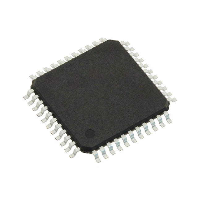
XC2C32A-4VQG44C
IC CPLD 32MC 3.8NS 44VQFP


Compare
$11.02
Price update:2024-05-06
Available in stock:
79


45
Serves customers in 45 countries
1000+
Worldwide Manufacturers
$140M
$140M Growth in 5 Years
50.0M+
50M Parts Shipped in 5 Years

Xilinx
Xilinx stands as a preeminent purveyor of All Programmable Field-Programmable Gate Arrays (FPGAs), System on Chips (SoCs), Multiprocessor System on Chips (MPSoCs), and Three-Dimensional Integrated Circuits (3D ICs). AMD stands in a distinctive position, facilitating applications that embody a dual nature of software-defined sophistication and hardware-honed optimization. This empowering of industries finds its zenith in the realms of Cloud Computing, 5G Wireless Connectivity, Embedded Vision, and the sprawling domain of Industrial Internet of Things (IIoT).
View All Product from Xilinx


The CoolRunner-II 128-macrocell device is designed for both high performance and low power applications. This lends power savings to high-end communication equipment and high speed to battery operated devices. Due to the low power stand-by and dynamic operation, overall system reliability is improved
This device consists of eight Function Blocks inter-connected by a low power Advanced Interconnect Matrix (AIM). The AIM feeds 40 true and complement inputs to each Function Block. The Function Blocks consist of a 40 by 56 P-term PLA and 16 macrocells which contain numerous configuration bits that allow for combinational or registered modes of operation.
Additionally, these registers can be globally reset or preset and configured as a D or T flip-flop or as a D latch. There are also multiple clock signals, both global and local product term types, configured on a per macrocell basis. Output pin configurations include slew rate limit, bus hold, pull-up, open drain and programmable grounds. A Schmitt-trigger input is available on a per input pin basis. In addition to storing macrocell output states, the macrocell registers may be configured as direct input registers to store signals directly from input pins.
Clocking is available on a global or Function Block basis. Three global clocks are available for all Function Blocks as a synchronous clock source. Macrocell registers can be individually configured to power up to the zero or one state. A global set/reset control line is also available to asynchronously set or reset selected registers during operation. Additional local clock, synchronous clock-enable, asynchronous set/reset and output enable signals can be formed using product terms on a per-macrocell or per-Function Block basis.
A DualEDGE flip-flop feature is also available on a per macrocell basis. This feature allows high performance synchronous operation based on lower frequency clocking to help reduce the total power consumption of the device.
Circuitry has also been included to divide one externally supplied global clock (GCK2) by eight different selections. This yields divide by even and odd clock frequencies.
The use of the clock divide (division by 2) and DualEDGE flip-flop gives the resultant CoolCLOCK feature
DataGATE is a method to selectively disable inputs of the CPLD that are not of interest during certain points in time.
By mapping a signal to the DataGATE function, lower power can be achieved due to reduction in signal switching.
Another feature that eases voltage translation is I/O banking. Two I/O banks are available on the CoolRunner-II 128 macrocell device that permit easy interfacing to 3.3V, 2.5V, 1.8V, and 1.5V devices.
The CoolRunner-II 128 macrocell CPLD is I/O compatible with various JEDEC I/O standards (see Table 1). This device is also 1.5V I/O compatible with the use of Schmitt-trigger inputs.
Table 1: I/O Standards for XC2C128(1)
IOSTANDARD AttributeOutput VCCIOInput VCCIOInput VREFBoard Termination Voltage VTTLVTTL3.33.3N/AN/ALVCMOS333.33.3N/AN/ALVCMOS252.52.5N/AN/ALVCMOS181.81.8N/AN/ALVCMOS15(2)1.51.5N/AN/AHSTL_11.51.50.750.75SSTL2_12.52.51.251.25SSTL3_13.33.31.51.5Feature
• In-System Programmable PROMs for Configuration of Xilinx® FPGAs
• Low-Power Advanced CMOS NOR Flash Process
• Endurance of 20,000 Program/Erase Cycles
• Operation over Full Industrial Temperature Range (–40°C to +85°C)
• IEEE Standard 1149.1/1532 Boundary-Scan (JTAG) Support for Programming, Prototyping, and Testing
• JTAG Command Initiation of Standard FPGA Configuration


Product Attributes
| TYPE | DESCRIPTION | Select all |
|---|---|---|
| Package / Case | 44-TQFP | |
| Programmable | Verified | |
| Supplier Device Package | 44-VQFP (10x10) | |
| Programmable Type | In System Programmable | |
| Delay Time tpd(1) Max | 3.8 ns | |
| Voltage Supply - Internal | 1.7V ~ 1.9V | |
| Number of Logic Elements/Blocks | 2 | |
| Number of Macrocells | 32 | |
| Number of Gates | 750 | |
| Number of I/O | 33 | |
| Series | CoolRunner II | |
| Operating Temperature | 0°C ~ 70°C (TA) | |
| Package | Tray | |
| Mounting Type | Surface Mount | |
| Product Status | Active |
Blog


 Unveiling the Future: The Surge of Microcontrollers in 2024In the dynamic world of electronic components, microcontrollers stand out as a testament to innovation and versatility. As we edge closer to 2024, the landscape for microcontrollers and semiconductors, spearheaded by giants like STMicroelectronics, Texas Instruments, and Microchip, is set for remarkable transformation.
 Microcontrollers vs. Microprocessors: Unveiling the Core Differences for Embedded Systems EngineeringSeasoned professionals in the realm of embedded systems engineering and product development within the electronics sphere often grapple with distinguishing between microcontrollers and microprocessors. Despite their foundational role in the design and fabrication of a myriad of electronic gadgets, understanding their unique functionalities based on mere definitions can be challenging:
 A Deep Dive into the Global Ceramic Capacitors MarketJoin us in exploring the emerging subplot of environmental consciousness within the global ceramic capacitors market.
 Mastering Current Measurement with MicrocontrollersUnlock precise current measurement secrets with Microcontrollers! Conquer challenges, meet superhero solutions, and revolutionize accuracy with on-chip Analog Core Independent Peripherals (CIPs).
 What is a Rectifier Diode: A Guide to BeginnersMeet the unsung heroes of electronics—Rectifier Diodes! Explore their magic, applications, and join the behind-the-scenes adventure into gadget power.


$11.02
Price update:2024-05-06
Available in stock:
79
Xilinx
Xilinx stands as a preeminent purveyor of All Programmable Field-Programmable Gate Arrays (FPGAs), System on Chips (SoCs), Multiprocessor System on Chips (MPSoCs), and Three-Dimensional Integrated Circuits (3D ICs). AMD stands in a distinctive position, facilitating applications that embody a dual nature of software-defined sophistication and hardware-honed optimization. This empowering of industries finds its zenith in the realms of Cloud Computing, 5G Wireless Connectivity, Embedded Vision, and the sprawling domain of Industrial Internet of Things (IIoT).
View All Product from XilinxBlog
- Unveiling the Future: The Surge of Microcontrollers in 2024In the dynamic world of electronic components, microcontrollers stand out as a testament to innovation and versatility. As we edge closer to 2024, the landscape for microcontrollers and semiconductors, spearheaded by giants like STMicroelectronics, Texas Instruments, and Microchip, is set for remarkable transformation.
- Microcontrollers vs. Microprocessors: Unveiling the Core Differences for Embedded Systems EngineeringSeasoned professionals in the realm of embedded systems engineering and product development within the electronics sphere often grapple with distinguishing between microcontrollers and microprocessors. Despite their foundational role in the design and fabrication of a myriad of electronic gadgets, understanding their unique functionalities based on mere definitions can be challenging:
- A Deep Dive into the Global Ceramic Capacitors MarketJoin us in exploring the emerging subplot of environmental consciousness within the global ceramic capacitors market.
- Mastering Current Measurement with MicrocontrollersUnlock precise current measurement secrets with Microcontrollers! Conquer challenges, meet superhero solutions, and revolutionize accuracy with on-chip Analog Core Independent Peripherals (CIPs).
- What is a Rectifier Diode: A Guide to BeginnersMeet the unsung heroes of electronics—Rectifier Diodes! Explore their magic, applications, and join the behind-the-scenes adventure into gadget power.
Popular Manufacturers
View all manufactures More


Popular Parts Number
More Electronic Parts MoreXC2C32A-4VQG44C
IC CPLD 32MC 3.8NS 44VQFP
XCR3064XL-10VQG44C
IC CPLD 64MC 9.1NS 44VQFP
XC2C256-7FTG256C
IC CPLD 256MC 6.7NS 256FTBGA

XC9572XL-10VQG64I
IC CPLD 72MC 10NS 64VQFP
XC2C256-7VQG100I
IC CPLD 256MC 6.7NS 100VQFP
XC9536XL-7VQG64C
IC CPLD 36MC 7.5NS 64VQFP
XC2C32A-6CP56C
IC CPLD 32MC 5.5NS 56CSBGA

XC9536XL-10VQ64I
IC CPLD 36MC 10NS 64VQFP

XCR3032XL-10VQ44C
IC CPLD 32MC 9.1NS 44VQFP
XC9536XL-7CSG48I
IC CPLD 36MC 7.5NS 48CSBGA