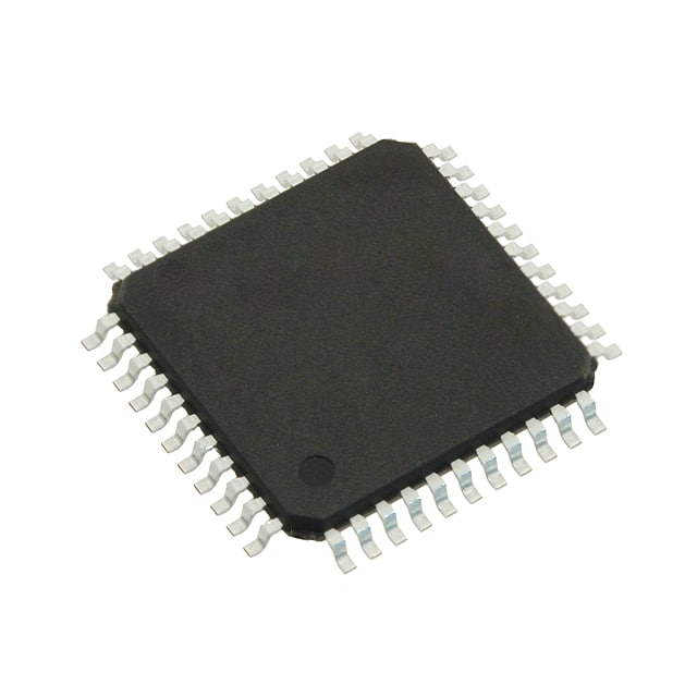
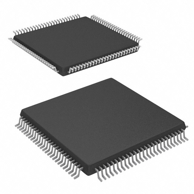
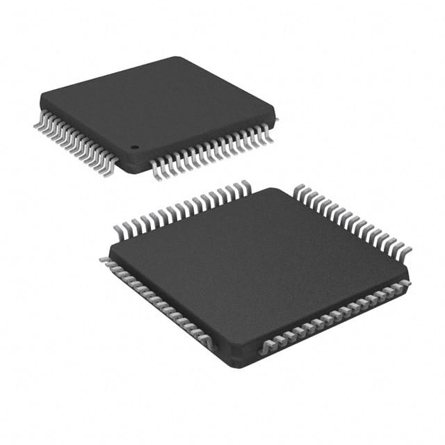
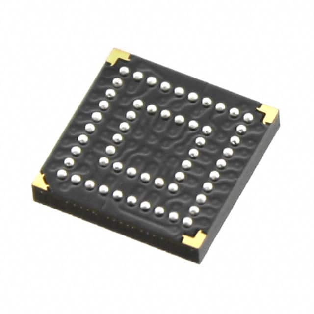
XCR3256XL-12TQG144I
Compare
XCR3256XL-12TQG144I
IC CPLD 256MC 10.8NS 144TQFP


Compare
$55.12
Price update:2024-05-23
Available in stock:
500


45
Serves customers in 45 countries
1000+
Worldwide Manufacturers
$140M
$140M Growth in 5 Years
50.0M+
50M Parts Shipped in 5 Years

Xilinx
Xilinx stands as a preeminent purveyor of All Programmable Field-Programmable Gate Arrays (FPGAs), System on Chips (SoCs), Multiprocessor System on Chips (MPSoCs), and Three-Dimensional Integrated Circuits (3D ICs). AMD stands in a distinctive position, facilitating applications that embody a dual nature of software-defined sophistication and hardware-honed optimization. This empowering of industries finds its zenith in the realms of Cloud Computing, 5G Wireless Connectivity, Embedded Vision, and the sprawling domain of Industrial Internet of Things (IIoT).
View All Product from Xilinx


Introduction
The Spartan@-ll Field-Programmable Gate Array family gives users high performance, abundant logic resources, and a rich feature set, all at an exceptionally low price. The six-member family offers densities ranging from 15,000 to 200,000 system gates, as shown in Table 1. System performance is supported up to 200 MHz. Features includeblock RAM(to 56K bits), distributed RAM(to 75,264 bits), 16 selectable I/O standards, and four DLLs. Fast, predictable interconnect means that successive design iterations continue to meet timing requirements.
The Spartan-lI family is a superior alternative to mask-programmed ASICs. The FPGA avoids the initial cost, lengthy development cycles, and inherent risk ofconventional ASICs. Also, FPGA programmability permits design upgrades in the field with no hardware replacement necessary(impossible with ASICs).
Features
· Second generation ASIC replacement technology
-Densities as high as 5,292 logic cells with up to 200,000 system gates
-Streamlined features based on Virtex? FPGA architecture
-Unlimited reprogrammability
-Very low cost
-Cost-effective 0.18 micron process
· System level features
-SelectRAM TM hierarchical memory: 16bits/LUT distributed RAM Configurable 4K bit block RAM
· Fast interfaces to external RAM
-Fully PCI compliant
-Low-power segmented routing architecture
-Full readback ability for verification/observability
-Dedicated carry logic for high-speed arithmetic
-Efficient multiplier support
-Cascade chain for wide-input functions
-Abundant registers/latches with enable, set, reset
-Four dedicated DLLs for advanced clock control
-Four primary low-skew global clock distribution nets
-IEEE 1149.1 compatible boundary scan logic
·Versatile I/O and packaging
-Pb-free package options
-Low-cost packages available in all densities
-Family footprint compatibility in common packages
-16high-performance interface standards
-Hot swap Compact PCI friendly
-Zero hold time simplifies system timing
·Core logic powered at 2.5V and I/Os powered at 1.5V,2.5V,or 3.3V
·Fully supported by powerful XilinxISEdevelopment system
-Fully automatic mapping,placement,and routing
Feature
- Low power 3.3V 256 macrocell CPLD
- 7.0 ns pin-to-pin logic delays
- System frequencies up to 154 MHz
- 256 macrocells with 6,000 usable gates
- Available in small footprint packages
- 144-pin TQFP (120 user I/O pins)
- 208-pin PQFP (164 user I/O)
- 256-ball FBGA (164 user I/O)
- 280-ball CS BGA (164 user I/O)
- Optimized for 3.3V systems
- Ultra low power operation
- Typical Standby Current of 18 μA at 25° C
- 5V tolerant I/O pins with 3.3V core supply
- Advanced 0.35 micron five layer metal EEPROM process
- Fast Zero Power™ (FZP) CMOS design technology
- 3.3V PCI electrical specification compatible outputs (no internal clamp diode on any input or I/O)
- Advanced system features
- In-system programming
- Input registers
- Predictable timing model
- Up to 23 clocks available per function block
- Excellent pin retention during design changes
- Full IEEE Standard 1149.1 boundary-scan (JTAG)
- Four global clocks
- Eight product term control terms per function block
- Fast ISP programming times
- Port Enable pin for additional I/O
- 2.7V to 3.6V supply voltage at industrial grade voltage range
- Programmable slew rate control per output
- Security bit prevents unauthorized access
- Refer to the CoolRunner™ XPLA3 family data sheet (DS012) for architecture description


Related Products
| Mfr Part # | Price ($) | Quantity Available | |
|---|---|---|---|
 XCR3256XL-12FTG256CIC CPLD 256MC 10.8NS 256FTBGA | 68.90 |
17
Marketplace | |
 XCR3256XL-12PQ208CIC CPLD 256MC 10.8NS 208QFP | 413.40 |
298
Marketplace | |
 XCR3256XL-12TQ144CIC CPLD 256MC 10.8NS 144TQFP | 55.12 |
12
Marketplace | |
 XCR3256XL-10TQG144IIC CPLD 256MC 9.1NS 144TQFP | 41.34 |
3082
Marketplace | |
 XCR3256XL-12FT256IIC CPLD 256MC 10.8NS 256FTBGA | 20.67 |
320
Marketplace |
Product Attributes
| TYPE | DESCRIPTION | Select all |
|---|---|---|
| Package / Case | 144-LQFP | |
| Programmable | Not Verified | |
| Supplier Device Package | 144-TQFP (20x20) | |
| Programmable Type | In System Programmable (min 1K program/erase cycles) | |
| Delay Time tpd(1) Max | 10.8 ns | |
| Voltage Supply - Internal | 2.7V ~ 3.6V | |
| Number of Logic Elements/Blocks | 16 | |
| Number of Macrocells | 256 | |
| Number of Gates | 6000 | |
| Number of I/O | 120 | |
| Series | CoolRunner XPLA3 | |
| Operating Temperature | -40°C ~ 85°C (TA) | |
| Package | Tray | |
| Mounting Type | Surface Mount | |
| Product Status | Active |
Blog


 Unveiling the Future: The Surge of Microcontrollers in 2024In the dynamic world of electronic components, microcontrollers stand out as a testament to innovation and versatility. As we edge closer to 2024, the landscape for microcontrollers and semiconductors, spearheaded by giants like STMicroelectronics, Texas Instruments, and Microchip, is set for remarkable transformation.
 Microcontrollers vs. Microprocessors: Unveiling the Core Differences for Embedded Systems EngineeringSeasoned professionals in the realm of embedded systems engineering and product development within the electronics sphere often grapple with distinguishing between microcontrollers and microprocessors. Despite their foundational role in the design and fabrication of a myriad of electronic gadgets, understanding their unique functionalities based on mere definitions can be challenging:
 A Deep Dive into the Global Ceramic Capacitors MarketJoin us in exploring the emerging subplot of environmental consciousness within the global ceramic capacitors market.
 Mastering Current Measurement with MicrocontrollersUnlock precise current measurement secrets with Microcontrollers! Conquer challenges, meet superhero solutions, and revolutionize accuracy with on-chip Analog Core Independent Peripherals (CIPs).
 What is a Rectifier Diode: A Guide to BeginnersMeet the unsung heroes of electronics—Rectifier Diodes! Explore their magic, applications, and join the behind-the-scenes adventure into gadget power.


$55.12
Price update:2024-05-23
Available in stock:
500
Xilinx
Xilinx stands as a preeminent purveyor of All Programmable Field-Programmable Gate Arrays (FPGAs), System on Chips (SoCs), Multiprocessor System on Chips (MPSoCs), and Three-Dimensional Integrated Circuits (3D ICs). AMD stands in a distinctive position, facilitating applications that embody a dual nature of software-defined sophistication and hardware-honed optimization. This empowering of industries finds its zenith in the realms of Cloud Computing, 5G Wireless Connectivity, Embedded Vision, and the sprawling domain of Industrial Internet of Things (IIoT).
View All Product from XilinxBlog
- Unveiling the Future: The Surge of Microcontrollers in 2024In the dynamic world of electronic components, microcontrollers stand out as a testament to innovation and versatility. As we edge closer to 2024, the landscape for microcontrollers and semiconductors, spearheaded by giants like STMicroelectronics, Texas Instruments, and Microchip, is set for remarkable transformation.
- Microcontrollers vs. Microprocessors: Unveiling the Core Differences for Embedded Systems EngineeringSeasoned professionals in the realm of embedded systems engineering and product development within the electronics sphere often grapple with distinguishing between microcontrollers and microprocessors. Despite their foundational role in the design and fabrication of a myriad of electronic gadgets, understanding their unique functionalities based on mere definitions can be challenging:
- A Deep Dive into the Global Ceramic Capacitors MarketJoin us in exploring the emerging subplot of environmental consciousness within the global ceramic capacitors market.
- Mastering Current Measurement with MicrocontrollersUnlock precise current measurement secrets with Microcontrollers! Conquer challenges, meet superhero solutions, and revolutionize accuracy with on-chip Analog Core Independent Peripherals (CIPs).
- What is a Rectifier Diode: A Guide to BeginnersMeet the unsung heroes of electronics—Rectifier Diodes! Explore their magic, applications, and join the behind-the-scenes adventure into gadget power.
Popular Manufacturers
View all manufactures More


Popular Parts Number
More Electronic Parts MoreXCR3256XL-12TQG144I
IC CPLD 256MC 10.8NS 144TQFP
XCR3064XL-10VQG44C
IC CPLD 64MC 9.1NS 44VQFP

XC9572XL-10VQG64I
IC CPLD 72MC 10NS 64VQFP
XC2C256-7VQG100I
IC CPLD 256MC 6.7NS 100VQFP
XC9536XL-7VQG64C
IC CPLD 36MC 7.5NS 64VQFP
XC2C32A-6CP56C
IC CPLD 32MC 5.5NS 56CSBGA

XC9536XL-10VQ64I
IC CPLD 36MC 10NS 64VQFP

XCR3032XL-10VQ44C
IC CPLD 32MC 9.1NS 44VQFP
XC9536XL-7CSG48I
IC CPLD 36MC 7.5NS 48CSBGA

XCR3032XL-10CSG48I
IC CPLD 32MC 9.1NS 48CSBGA